


 Trouble in Your Tank: Understanding Interconnect Defects, Part 1
 It’s Only Common Sense: Marketing Isn’t Fluff, It’s Ammunition
 Driving Innovation: Mechanical and Optical Processes During Rigid-flex Production


Scientists Boost Stability of Low-Cost, Large-Area Solar Modules
January 23, 2019 | OISTEstimated reading time: 3 minutes
Scientists at the Okinawa Institute of Science and Technology Graduate University (OIST) have resolved a fundamental weakness in a promising solar technology known as Perovskite Solar Cells, or PSCs. Their innovations appear to improve both the devices’ stability and scalability in one fell swoop and could be key to moving PSCs to market.
Third-generation solar cells efficiently convert sunlight into usable electricity and cost less energy to manufacture than old-school silicon cells. PSCs, in particular, have garnered the attention of science and industry thanks to their low cost and high efficiency. Though their performance is promising in lab tests, the devices still suffer from low stability and cannot be produced commercially until they’re built to last.
“We need solar modules that can last for at least 5 to 10 years. For now, the lifetime of PSCs is much shorter,” said Dr. Longbin Qiu, first author of the paper and a postdoctoral scholar in the OIST Energy Materials and Surface Sciences Unit, led by Prof. Yabing Qi.
The study, published online in Advanced Functional Materials on December 13, 2018, supports prior evidence that a commonly used material in PSCs, called titanium dioxide, degrades the devices and limits their lifetime. The researchers replaced this material with tin dioxide, a stronger conductor without these degrading properties. They optimized their method of applying tin dioxide to produce stable, efficient and scalable PSCs.
In experiments, the researchers found that tin dioxide-based devices showed lifetimes over three times longer than PSC devices using titanium dioxide. “Tin dioxide can give users the device performance they need,” said Qiu.
An Improved Design
PSCs consist of layered materials, each with a specific function. The “active layer,” made from perovskite materials, absorbs incoming sunlight in the form of particles called photons. When a photon strikes a solar cell, it generates negatively-charged electrons and positively-charged holes in the active layer. Scientists control the flow of these electrons and holes by sandwiching the active layer between two “transport materials,” thus creating a built-in electrical field.
To help usher electrons in the right direction, many PSCs include an “electron transport layer.” Most PSCs employ titanium dioxide as their electron transport layer, but when exposed to sunlight, the material reacts with perovskite and ultimately degrades the device. Tin dioxide stands as a viable replacement for titanium dioxide, but before this study, it had not been successfully incorporated into a large-scale device.
Using a common technique in the industry called sputtering deposition, the researchers learned how to craft an effective electron transport layer from tin dioxide. Sputtering deposition works by bombarding the target material, here tin dioxide, with charged particles, causing it to spray upwards onto a waiting surface. By precisely controlling the power of the sputtering and speed of the deposition, the researchers produced smooth layers with a uniform thickness over a large area.
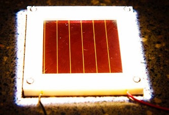
*Their new solar cells achieved an efficiency of over 20%. To demonstrate the scalability of this new method, the researchers then fabricated 5 by 5 centimeter solar modules with a designated area of 22.8 square-centimeters, finding that the resulting devices showed over 12% efficiency. This research, which was supported by the OIST Technology Development and Innovation Center’s Proof-of-Concept Program, represents a crucial step forward towards meeting the current industry standard for PSC efficiency.
Dr. Longbin Qiu holds up a sheet of solar cells made from flexible materials. The Energy Materials and Surface Sciences Unit aims to develop these devices to craft solar curtains and solar technologies that can be easily incorporated into people’s homes.
Moving to Market
The researchers plan to continue optimizing their PSC design with the goal of producing large-scale solar modules with improved efficiency. The research unit experiments with flexible, transparent solar devices and aims to apply their optimized PSC design in solar windows, curtains, backpacks and deployable charging units.
“We want to scale these devices up to a large size, and though their efficiency is already reasonable, we want to push it further,” said Prof. Qi. “We are optimistic that in the next few years, this technology will be viable for commercialization.”
Share on:


Testimonial
"Our marketing partnership with I-Connect007 is already delivering. Just a day after our press release went live, we received a direct inquiry about our updated products!"
Rachael Temple - AlltematedSuggested Items
SEMI Foundation Honors Applied Materials at SEMICON West with 2025 Excellence in Achievement Award for Talent Development
11/04/2025 | SEMIThe SEMI Foundation announced it recognized Applied Materials, Inc. with the Excellence in Achievement Award at SEMICON West 2025 in Phoenix, Arizona, honoring the company’s outstanding leadership and collaboration in building the next generation of semiconductor talent.
On the Line With… Ultra HDI, Episode 8: “Materials, Up and Coming Capabilities,” Now Available
11/05/2025 | I-Connect007I-Connect007 is excited to announce the release of the eighth episode of its 12-part podcast series, On the Line With… American Standard Circuits: Ultra HDI. In this episode, “Materials, Up and Coming Capabilities,” host Nolan Johnson sits down with resident expert John Johnson, Director of Quality and Advanced Technology at American Standard Circuits, to discuss how material selection influences the Ultra HDI (UHDI) manufacturing process.
New Podcast Episode: “Bonding Innovation: How Adhesives and Coatings Are Powering the Next Generation of Electronics”
11/05/2025 | I-Connect007I-Connect007 has released of a new episode in its Voices of the Industry podcast series, titled “Bonding Innovation: How Adhesives and Coatings Are Powering the Next Generation of Electronics.” Hosted by Nolan Johnson, this insightful discussion dives deep into the evolving world of adhesives and coatings—materials that are redefining performance, reliability, and design in modern electronics manufacturing. Dymax's Doug Katze, a leading expert in adhesive technologies, delivers what can only be described as a master class on how these critical materials are adapting to meet rapidly changing market demands.
Sealed for Survival: Potting Electronics for the Toughest Environments
10/29/2025 | Beth Massey, MacDermid Alpha Electronics SolutionsElectronics deployed in harsh conditions face relentless threats from vibration, impact, chemical contaminants, airborne pollutants, and moisture, conditions that can quickly lead to failure without robust protection. Potting, the process of encapsulating electronics in a protective polymer, is a widely used strategy to safeguard devices from both environmental and mechanical hazards.
Driving Innovation: Mechanical and Optical Processes During Rigid-flex Production
10/28/2025 | Kurt Palmer -- Column: Driving InnovationRigid-flex printed circuit boards are a highly effective solution for placing complex circuitry in tight, three-dimensional spaces. They are now indispensable across a range of industries, from medical devices and aerospace to advanced consumer electronics, helping designers make the most efficient use of available space. However, their unique construction—combining rigid and flexible materials—presents a fundamental challenge for PCB manufacturers.