


 The Marketing Minute: Marketing With Layers
 The Right Approach: Electro-Tek—A Williams Family Legacy, Part 1
 It’s Only Common Sense: If You’re Not Differentiated, You’re Dead


New Technique Offers Rapid Assessment of Radiation Exposure
January 24, 2019 | NC State UniversityEstimated reading time: 2 minutes
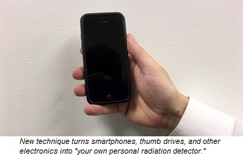
Researchers from North Carolina State University have developed a new technique that allows them to assess radiation exposure in about an hour using an insulator material found in most modern electronics. The technique can be used to triage medical cases in the event of a radiological disaster.
“If there is a large radiological event in a populated area, it would be difficult or impossible to treat everyone who could potentially have acute radiation syndrome,” says Robert Hayes, an associate professor of nuclear engineering at NC State and first author of a paper on the work. “You’d need to be able to figure out who was exposed to enough radiation to require treatment.”
The approach relies on testing crystalline insulators found in everything from thumb drives to smartphones. Because the technique is high-throughput, accurate and precise, it can adequately assess an individual’s exposure in about an hour, Hayes says. Prior methods can take weeks.
“Given that health providers have a one- to two-week window to start treating victims of acute radiation syndrome, the technique should be sufficient to identify which patients require the necessary care,” Hayes says. “It could not only identify individual cases of acute radiation syndrome, but also help authorities determine which geographic areas received the most radiation.
“But it’s not just about identifying those that require care,” Hayes says. “For example, our technique might have been useful in a place like Fukushima, for putting people’s minds at ease. It’s like having your own personal radiation detector.”
The technique requires the insulator to be removed from its electronic device and cleaned. The sample is then placed in a thermally stimulated luminescence reader, which collects spectra relating to the number of electrons found in the flaws inherent to the sample’s crystalline structure. That spectral data is then fed into a custom algorithm that calculates the sample’s radiation exposure.
“This technique requires specialized equipment and expertise, so it’s not something most locales would have on hand,” Hayes says. “But labs like mine could run the tests and provide the authorities with good data very quickly. In addition to NC State, I know there’s another lab with relevant expertise and infrastructure at Oklahoma State University, and one in Denmark, though there are likely others.
“Hopefully, this technique won’t be necessary for a long time, if ever. But we think it’s important to develop these tools before they are needed.”
Share on:


Testimonial
"Your magazines are a great platform for people to exchange knowledge. Thank you for the work that you do."
Simon Khesin - Schmoll MaschinenSuggested Items
Samsung Cuts 2nm Wafer Prices to Undercut TSMC
09/30/2025 | I-Connect007 Editorial TeamSamsung Electronics has lowered the price of its 2-nanometer wafers to approximately $20,000, undercutting rival Taiwan Semiconductor Manufacturing Co. (TSMC) by about one-third, Digitimes reported on September 29.
Weaning the U.S. Military Off a Tablet Supply Chain That Leads to China
09/08/2025 | Jim Will, USPAETablet computers are essential to how our military fights, moves and sustains, but these devices are built on a fragile global supply chain with strong ties to China. Building domestic manufacturing to eliminate this vulnerability is feasible if we tap into the information and capabilities that already exist and create strong demand for tablets produced by trusted and assured sources.
Fresh PCB Concepts: Designing for Success at the Rigid-flex Transition Area
08/28/2025 | Team NCAB -- Column: Fresh PCB ConceptsRigid-flex PCBs come in all shapes and sizes. Manufacturers typically use fire-retardant, grade 4 (FR-4) materials in the rigid section and flexible polyimide materials in the flex region. Because of the small size, some rigid-flex PCBs, like those for hearing aid devices, are among the most challenging to manufacture. However, regardless of its size, we should not neglect the transition area between the rigid and flexible material.
Semiconductors Get Magnetic Boost with New Method from UCLA Researchers
07/31/2025 | UCLA NewsroomA new method for combining magnetic elements with semiconductors — which are vital materials for computers and other electronic devices — was unveiled by a research team led by the California NanoSystems Institute at UCLA.
Japan’s OHISAMA Project Aims to Beam Solar Power from Space This Year
07/14/2025 | I-Connect007 Editorial TeamJapan could be on the cusp of making history with its OHISAMA project in its quest to become the first country to transmit solar power from space to Earth, The Volt reported.