


 The Marketing Minute: Marketing With Layers
 The Right Approach: Electro-Tek—A Williams Family Legacy, Part 1
 It’s Only Common Sense: If You’re Not Differentiated, You’re Dead


Unlocking Graphene’s Superconducting Powers with a Twist and a Squeeze
January 25, 2019 | Columbia UniversityEstimated reading time: 3 minutes
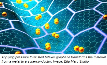
Graphene has been heralded as a wonder material. Not only is it the strongest, thinnest material ever discovered, its exceptional ability to conduct heat and electricity paves the way for innovation in areas ranging from electronics to energy to medicine.
Now, a Columbia University-led team has developed a new method to finely tune adjacent layers of graphene—lacy, honeycomb-like sheets of carbon atoms—to induce superconductivity. Their research provides new insights into the physics underlying this two-dimensional material’s intriguing characteristics.
“Our work demonstrates new ways to induce superconductivity in twisted bilayer graphene, in particular, achieved by applying pressure,” said Cory Dean, assistant professor of physics at Columbia and the study’s principal investigator. “It also provides critical first confirmation of last year’s MIT results—that bilayer graphene can exhibit electronic properties when twisted at an angle—and furthers our understanding of the system, which is extremely important for this new field of research.”
In March 2018 researchers at the Massachusetts Institute of Technology reported a groundbreaking discovery that two graphene layers can conduct electricity without resistance when the twist angle between them is 1.1 degrees, referred to as the “magic angle.”
But hitting that magic angle has proven difficult. “The layers must be twisted to within roughly a tenth of a degree around 1.1, which is experimentally challenging,” Dean said. “We found that very small errors in alignment could give entirely different results.”
So Dean and his colleagues, who include scientists from the National Institute for Materials Science and the University of California, Santa Barbara, set out to test whether magic-angle conditions could be achieved at bigger rotations.
“Rather than trying to precisely control the angle, we asked whether we could instead vary the spacing between the layers,” said Matthew Yankowitz, a postdoctoral research scientist in Columbia’s physics department and first author on the study. “In this way any twist angle could, in principle, be turned into a magic angle.”
They studied a sample with twist angle of 1.3 degrees—only slightly larger than the magic angle but far enough away to preclude superconductivity. Applying pressure transformed the material from a metal into either an insulator—in which electricity cannot flow—or a superconductor—where electrical current can pass without resistance—depending on the number of electrons in the material.
“Remarkably, by applying pressure of over 10,000 atmospheres we observe the emergence of the insulating and superconducting phases,” Dean said. Additionally, the superconductivity develops at the highest temperature observed in graphene so far, just over 3 degrees above absolute zero.”
To reach the high pressures needed to induce superconductivity the team worked closely with the National High Magnetic Field user facility, known as the Maglab, in Tallahassee, Florida. “This effort was a huge technical challenge,” says Dean. “After fabricating one of most unique devices we’ve ever worked with, we then had to combine cryogenic temperatures, high magnetic fields, and high pressure – all while measuring electrical response. Putting this all together was a daunting task and our ability to make it work is really a tribute to the fantastic expertise at the Maglab.”
The researchers believe it may be possible to enhance the critical temperature of the superconductivity further at even higher pressures. The ultimate goal is to one day develop a superconductor which can perform under room temperature conditions, and although this may prove challenging in graphene, it could serve as a roadmap for achieving this goal in other materials.
Andrea Young, assistant professor of physics at UC Santa Barbara, a collaborator on the study, said the work clearly demonstrates that squeezing the layers has same effect as twisting them and offers an alternative paradigm for manipulating the electronic properties in graphene.
“Our findings significantly relax the constraints that make it challenging to study the system and gives us new knobs to control it,” Young said.
Dean and Young are now twisting and squeezing a variety of atomically-thin materials in the hopes of finding superconductivity emerging in other two-dimensional systems.
“Understanding ‘why’ any of this is happening is a formidable challenge but critical for eventually harnessing the power of this material—and our work starts unraveling the mystery,’” Dean said.
—By Carla Cantor
Share on:


Testimonial
"In a year when every marketing dollar mattered, I chose to keep I-Connect007 in our 2025 plan. Their commitment to high-quality, insightful content aligns with Koh Young’s values and helps readers navigate a changing industry. "
Brent Fischthal - Koh YoungSuggested Items
Samsung Cuts 2nm Wafer Prices to Undercut TSMC
09/30/2025 | I-Connect007 Editorial TeamSamsung Electronics has lowered the price of its 2-nanometer wafers to approximately $20,000, undercutting rival Taiwan Semiconductor Manufacturing Co. (TSMC) by about one-third, Digitimes reported on September 29.
Weaning the U.S. Military Off a Tablet Supply Chain That Leads to China
09/08/2025 | Jim Will, USPAETablet computers are essential to how our military fights, moves and sustains, but these devices are built on a fragile global supply chain with strong ties to China. Building domestic manufacturing to eliminate this vulnerability is feasible if we tap into the information and capabilities that already exist and create strong demand for tablets produced by trusted and assured sources.
Fresh PCB Concepts: Designing for Success at the Rigid-flex Transition Area
08/28/2025 | Team NCAB -- Column: Fresh PCB ConceptsRigid-flex PCBs come in all shapes and sizes. Manufacturers typically use fire-retardant, grade 4 (FR-4) materials in the rigid section and flexible polyimide materials in the flex region. Because of the small size, some rigid-flex PCBs, like those for hearing aid devices, are among the most challenging to manufacture. However, regardless of its size, we should not neglect the transition area between the rigid and flexible material.
Semiconductors Get Magnetic Boost with New Method from UCLA Researchers
07/31/2025 | UCLA NewsroomA new method for combining magnetic elements with semiconductors — which are vital materials for computers and other electronic devices — was unveiled by a research team led by the California NanoSystems Institute at UCLA.
Japan’s OHISAMA Project Aims to Beam Solar Power from Space This Year
07/14/2025 | I-Connect007 Editorial TeamJapan could be on the cusp of making history with its OHISAMA project in its quest to become the first country to transmit solar power from space to Earth, The Volt reported.