


 The Marketing Minute: Marketing With Layers
 The Right Approach: Electro-Tek—A Williams Family Legacy, Part 1
 It’s Only Common Sense: If You’re Not Differentiated, You’re Dead


Breakthrough Reported in Fabricating Nanochips
January 25, 2019 | NYU TandonEstimated reading time: 3 minutes
An international team of researchers has reported a breakthrough in fabricating atom-thin processors — a discovery that could have far-reaching impacts on nanoscale chip production and in labs across the globe where scientists are exploring 2D materials for ever-smaller and -faster semiconductors.
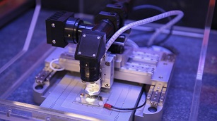
Elisa Riedo and doctoral student Xiangyu Liu fabricate high-quality 2D chipsThey demonstrate that lithography using a probe heated above 100 degrees Celsius outperformed standard methods for fabricating metal electrodes on 2D semiconductors such as molybdenum disulfide (MoS₂). Such transitional metals are among the materials that scientists believe may supplant silicon for atomically small chips. The team’s new fabrication method — called thermal scanning probe lithography (t-SPL) — offers a number of advantages over today’s electron beam lithography (EBL).
First, thermal lithography significantly improves the quality of the 2D transistors, offsetting the Schottky barrier, which hampers the flow of electrons at the intersection of metal and the 2D substrate. Also, unlike EBL, the thermal lithography allows chip designers to easily image the 2D semiconductor and then pattern the electrodes where desired. Also, t-SPL fabrication systems promise significant initial savings as well as operational costs: They dramatically reduce power consumption by operating in ambient conditions, eliminating the need to produce high-energy electrons and to generate an ultra-high vacuum. Finally, this thermal fabrication method can be easily scaled up for industrial production by using parallel thermal probes.
Riedo expressed hope that t-SPL will take most fabrication out of scarce clean rooms — where researchers must compete for time with the expensive equipment — and into individual laboratories, where they might rapidly advance materials science and chip design. The precedent of 3D printers is an apt analogy: Someday these t-SPL tools with sub-10 nanometer resolution, running on standard 120-volt power in ambient conditions, could become similarly ubiquitous in research labs like hers.
“Patterning Metal Contacts on Monolayer MoS₂ with Vanishing Schottky Barriers Using Thermal Nanolithography” appears in the January 2019 edition of Nature Electronics with a “News & Views” analysis.
Riedo’s work on thermal probes dates back more than a decade, first with IBM Research - Zurich and subsequently SwissLitho, founded by former IBM researchers. A process based on a SwissLitho system was developed and used for the current research. She began exploring thermal lithography for metal nanomanufacturing at the City University of New York (CUNY) Graduate Center Advanced Science Research Center (ASRC), working alongside co-first-authors of the paper, Xiaorui Zheng and Annalisa Calò, who are now post-doctoral researchers at NYU Tandon; and Edoardo Albisetti, who worked on the Riedo team with a Marie Curie Fellowship.
Contributing authors include NYU Tandon Assistant Professor of Electrical and Computer Engineering Davood Shahrjerdi; NYU Tandon doctoral students Xiangyu Liu and Abdullah Sanad M. Alharbi; Columbia University’s Ghidewon Arefe, James Hone, Brian S. Lee, and Michal Lipson; Sungkyunkwan (Korea) University’s Xiaochi Liu and Won Jong Yoo; SwissLitho’s Martin Spieser; the Japanese National Institute of Materials Science’s Takashi Taniguchi and Kenji Watanabe; Italy’s National Research Council’s Carmela Aruta; and the Swiss École Polytechnique Fédérale de Lausanne’s Alberto Ciarrocchi and Andras Kis.
The research was supported by the U.S. Army Research Office, the Office of Basic Energy Sciences of the U.S. Department of Energy, the National Science Foundation, and the European Union’s Horizon 2020 Research and Innovation Programme.
About the New York University Tandon School of Engineering
The NYU Tandon School of Engineering dates to 1854, the founding date for both the New York University School of Civil Engineering and Architecture and the Brooklyn Collegiate and Polytechnic Institute (widely known as Brooklyn Poly). A January 2014 merger created a comprehensive school of education and research in engineering and applied sciences, rooted in a tradition of invention and entrepreneurship and dedicated to furthering technology in service to society. In addition to its main location in Brooklyn, NYU Tandon collaborates with other schools within NYU, one of the country’s foremost private research universities, and is closely connected to engineering programs at NYU Abu Dhabi and NYU Shanghai. It operates Future Labs focused on start-up businesses in downtown Manhattan and Brooklyn and an award-winning online graduate program.
Share on:


Testimonial
"We’re proud to call I-Connect007 a trusted partner. Their innovative approach and industry insight made our podcast collaboration a success by connecting us with the right audience and delivering real results."
Julia McCaffrey - NCAB GroupSuggested Items
ITW EAE Despatch Ovens Now Support ASTM 5423 Testing
10/15/2025 | ITW EAEAs the demand for high-performance electrical insulation materials continues to grow—driven by the rapid expansion of electric vehicles (EVs) and energy storage systems—thermal processing has become a critical step in material development.
Beyond Thermal Conductivity: Exploring Polymer-based TIM Strategies for High-power-density Electronics
10/13/2025 | Padmanabha Shakthivelu and Nico Bruijnis, MacDermid Alpha Electronics SolutionsAs power density and thermal loads continue to increase, effective thermal management becomes increasingly important. Rapid and efficient heat transfer from power semiconductor chip packages is essential for achieving optimal performance and ensuring long-term reliability of temperature-sensitive components. This is particularly crucial in power systems that support advanced applications such as green energy generation, electric vehicles, aerospace, and defense, along with high-speed computing for data centers and artificial intelligence (AI).
Is Glass Finally Coming of Age?
10/13/2025 | Nolan Johnson, I-Connect007Substrates, by definition, form the base of all electronic devices. Whether discussing silicon wafers for semiconductors, glass-and-epoxy materials in printed circuits, or the base of choice for interposers, all these materials function as substrates. While other substrates have come and gone, silicon and FR-4 have remained the de facto standards for the industry.
Creative Materials to Showcase Innovative Functional Inks for Medical Devices at COMPAMED 2025
10/09/2025 | Creative Materials, Inc.Creative Materials, a leading manufacturer of high-performance functional inks and coatings, is pleased to announce its participation in COMPAMED 2025, taking place November 17–20 in Düsseldorf, Germany.
Jiva Leading the Charge Toward Sustainable Innovation
09/30/2025 | Marcy LaRont, PCB007 MagazineEnvironmental sustainability in business—product circularity—is a high priority these days. “Circularity,” the term meant to replace “recycling,” in its simplest definition, describes a full circle life for electronic products and all their elements. The result is re-use or a near-complete reintroduction of the base materials back into the supply chain, leaving very little left for waste. For what cannot be reused productively, the ultimate hope is to have better, less harmful means of disposal and/or materials that can seamlessly and harmlessly decompose and integrate back into the natural environment. That is where Jiva and Soluboard come in.