


 Flexible Thinking: Designing Flex Circuits for Dynamic Reliability
 Global PCB Connections: Rigid-flex and Flexible PCBs—The Backbone of Modern Electronics
 Happy’s Tech Talk #29: Bend-to-Install Semi-flex FR-4


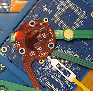
Laser Focus on Flex and Rigid-flex
January 28, 2019 | Barry Matties, I-Connect007Estimated reading time: 7 minutes
Noel: As we’ve said, yield is always a consideration. You have to be able to produce parts at a profit. We’ve had experiences even in the past few years where customers, OEMs, and producers have had to come to ESI for a solution where they thought they had another route to go, but were experiencing low yields in production. Again, with ESI’s laser material expertise, we’ve been able to help solve a lot of those problems.
Matties: When those types of customers come to you, what challenges do they face that they couldn’t solve? What was the problem?
Noel: It was the introduction of some of these 5G material sets. When utilizing traditional flex manufacturing processes that require high-temperature lamination, these new materials have a different glass transition temperature and also react differently to the other processing steps. That has led to yield loss. We’ve seen vias move out of pads and things like that. Being able to provide a solution to a customer that we can ensure them is an easier or more reliable process to do has been able to help solve those problems.
Matties: It goes right back to what you said about starting with collaboration up front. This is a great example of where that problem could have been avoided completely.
Noel: Absolutely. To be frank, we had already done the prework with some of these customers beforehand. It was an alternative process step that was readily available.
Ryder: I want to mention the base material manufacturers in this picture as well. ESI has always been close to the base material manufacturing world, and we continue to do so. We have constant discussions with the main material manufacturers so that when they introduce new materials, the process and the needs for the processability of the material is discussed. A perfect solution may not always be possible. The materials fit a certain performance that the OEMs need, but we do make it a point to be a part of that discussion with the material manufacturers.
Matties: Is there anything that we haven’t discussed that you feel we should include for the system designers?
Noel: One thing that ESI has been seeing is a continual press for increasingly smaller via sizes. When I started in flex 15 years ago, 100 microns was pretty standard. Now, we have customers pushing well below 40 microns. That’s a challenge for us and the customer not only for laser drilling but also for downstream and upstream processing. As we explore these smaller and smaller feature sizes, we need to evolve with the industry and provide solutions to that. That’s a big one.
Plate-ability is always a question. Again, compensating for upstream and downstream processes by utilizing a laser process that gives you the desired results is vital. ESI’s understanding of those processes is again a great part of our success and our customers’ success as well.
Ryder: I think that as the cost per photon decreases, we see laser-based manufacturing as a great opportunity for some of the new products coming on the market. We’d love to work closely with the industry and customers’ supply base to make that happen. We’re proud to be a part of it.
Matties: Thank you both for being here to share your thoughts, gentlemen.
Ryder: Thank you, Barry.
Noel: Thank you.
Page 2 of 2Share on:


Testimonial
"In a year when every marketing dollar mattered, I chose to keep I-Connect007 in our 2025 plan. Their commitment to high-quality, insightful content aligns with Koh Young’s values and helps readers navigate a changing industry. "
Brent Fischthal - Koh YoungSuggested Items
Nortech Systems Launches Power over Fiber Technology Platform for EMI-Sensitive Applications
04/08/2026 | Globe NewswireNortech Systems Incorporated, a leading provider of design and manufacturing solutions for complex electromedical devices and electromechanical systems, has announced the launch of its Power over Fiber technology platform.
Flexible Thinking: Designing Flex Circuits for Dynamic Reliability
04/09/2026 | Joe Fjelstad -- Column: Flexible ThinkingFlex circuits flex. No surprises there. However, they are also very commonly designed into products because they are thin and offer consistent thickness and dielectric properties, attributes highly prized by present-day product designers of personal electronics. This would include smartphones and, increasingly, wearable electronics for medical monitoring and even fashion.
Understanding Tolerances in Flexible Circuit Design
04/01/2026 | Chris Clark, Flexible Circuit TechnologiesThe challenge with cumulative tolerances is meeting the dimensional requirements for items dimensioned on a drawing or specification for a flexible or rigid-flex circuit. It is critical to understand the fabrication processes and how features are defined when creating your tolerance requirements.
Target Condition: An Exploration of Flooding PCB Layers
04/02/2026 | Kelly Dack -- Column: Target ConditionThe concept of flooding PCB layers with copper has been around for so long, you’d think we’d have it mastered. We haven’t. (Oh, and by “we,” I mean design engineers and the software tools we depend on.) Years ago, PCB artwork was created by hand using light tables, with tape applied to Mylar. Signals were slow, traces were relatively wide, and high-current paths were simply “beefed up” with wider copper. Signal integrity wasn’t yet a driving concern. Today, solid return paths are fundamental to robust design. We understand the importance of continuous reference planes for signal integrity and EMI control.
New, Greener Solutions for Etch: Novel Copper Extraction
03/30/2026 | Richard Nichols, GreenSource Engineering“Novel” is a typical marketing phrase that implies new and unique, but often “novel” actually means an established technology being applied to a new field or application. This, in turn, is often driven by newly relevant external motivation. GreenSource has been working on just such a solution: novel copper extraction, offering a better and greener alternative to traditional LLE control systems for cupric chloride etch.