


 American Made Advocacy: Smart Policies Can Ensure AI Data Centers Are Secure
 Beyond the Board: Early Engagement Means Faster Prototyping for Defense Programs
 Defense Speak Interpreted: The Autonomous Plane Battle—Skyborg Vs. Loyal Wingman


Metcal Robotic Soldering Reduces Risk, Increases Productivity
January 31, 2019 | MetcalEstimated reading time: 1 minute
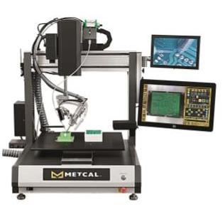
Metcal has launched the first robotic soldering system with its patented Connection Validation (CV) technology and a touchscreen graphical user interface to drastically mitigate the risk of solder joint defects and add productivity to the manufacturers' soldering process.
"The new CV Robotic Soldering System is the latest example of Metcal's industrial ingenuity," said Mak Manesh, global director, product management, for Metcal. "The system combines Metcal’s patented CV technology with a new graphical user interface."
CV reduces unnecessary dwell time by signalling to the system to move to the next solder joint in the program after a good joint is detected. The Metcal Robotic Soldering System comes with dual cameras, a touchscreen interface and powerful software, enabling easy programming and reduced turnover time.
Importing your Gerber or DXF file, or capturing the image of your printed circuit board, starts the programming process. Control of the system is integrated through the touchscreen interface, enabling users to select your solder joints, control the integrated solder feeder and manage process parameters through a graphical user interface.
About Metcal
Metcal is a benchtop solutions expert that has delivered broad value to customers since its Silicon Valley beginnings in 1982. Offering unrivalled performance, risk mitigation, and ROI, we give electronics manufacturers in automotive, aerospace, medical devices and military sectors the tools—and the confidence—they need to develop faster, safer, more advanced products. Metcal provides advanced technology products across hand soldering, convection rework, fume extraction, and fluid dispensing applications.
Share on:


Testimonial
"Our marketing partnership with I-Connect007 is already delivering. Just a day after our press release went live, we received a direct inquiry about our updated products!"
Rachael Temple - AlltematedSuggested Items
BTU International Earns 2025 Step-by-Step Excellence Award for Its Aqua Scrub™ Flux Management System
10/29/2025 | BTU International, Inc.BTU International, Inc., a leading supplier of advanced thermal processing equipment for the electronics manufacturing market, has been recognized with a 2025 Step-by-Step Excellence Award (SbSEA) for its Aqua Scrub™ Flux Management Technology, featured on the company’s Pyramax™ and Aurora™ reflow ovens.
On the Line With… Ultra HDI Podcast—Episode 7: “Solder Mask: Beyond the Traces,” Now Available
10/31/2025 | I-Connect007I-Connect007 is excited to announce the release of the seventh episode of its 12-part podcast series, On the Line With… American Standard Circuits: Ultra HDI. In this episode, “Solder Mask: Beyond the Traces,” host Nolan Johnson sits down with John Johnson, Director of Quality and Advanced Technology at American Standard Circuits, to explore the essential role that solder mask plays in the Ultra HDI (UHDI) manufacturing process.
Rehm Wins Mexico Technology Award for CondensoXLine with Formic Acid
10/17/2025 | Rehm Thermal SystemsModern electronics manufacturing requires technologies with high reliability. By using formic acid in convection, condensation, and contact soldering, Rehm Thermal Systems’ equipment ensures reliable, void-free solder joints — even when using flux-free solder pastes.
Indium Experts to Deliver Technical Presentations at SMTA International
10/14/2025 | Indium CorporationAs one of the leading materials providers to the power electronics assembly industry, Indium Corporation experts will share their technical insight on a wide range of innovative solder solutions at SMTA International (SMTAI), to be held October 19-23 in Rosemont, Illinois.
Knocking Down the Bone Pile: Revamp Your Components with BGA Reballing
10/14/2025 | Nash Bell -- Column: Knocking Down the Bone PileBall grid array (BGA) components evolved from pin grid array (PGA) devices, carrying over many of the same electrical benefits while introducing a more compact and efficient interconnect format. Instead of discrete leads, BGAs rely on solder balls on the underside of the package to connect to the PCB. In some advanced designs, solder balls are on both the PCB and the BGA package. In stacked configurations, such as package-on-package (PoP), these solder balls also interconnect multiple packages, enabling higher functionality in a smaller footprint.