


 Marcy’s Musings: Advancing the Advanced Materials Discussion
 The Marketing Minute: Cracking the Code of Technical Marketing
 Trouble in Your Tank: Implementing Direct Metallization in Advanced Substrate Packaging


Breakthrough in Understanding Electrical Conductivity in Doped Organic Semiconductors
February 1, 2019 | TU DresdenEstimated reading time: 2 minutes
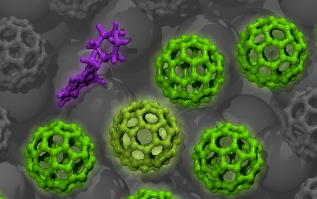
Researchers from the Dresden Integrated Center for Applied Physics and Photonic Materials (IAPP) and the Center for Advancing Electronics Dresden (cfaed) at TU Dresden, in cooperation with Stanford University (USA) and the Institute for Molecular Science in Okazaki (Japan), have identified the key parameters that influence electrical conductivity in doped organic conductors.
Organic semiconductors enable the fabrication of large-scale printed and mechanically flexible electronic applications, and have already successfully established themselves on the market for displays in the form of organic light-emitting diodes (OLEDs). In order to break into further market segments, however, improvements in performance are still needed. Doping is the answer. In semiconductor technology, doping refers to the targeted introduction of impurities (also called dopants) into the semiconductor material of an integrated circuit. These dopants function as intentional "disturbances" in the semiconductor that can be used to specifically control the behaviour of the charge carriers and thus the electrical conductivity of the original material. Even the smallest amounts of these can have a very strong influence on electrical conductivity. Molecular doping is an integral part of the majority of commercial organic electronics applications. Until now, however, an insufficient fundamental physical understanding of the transport mechanisms of charges in doped organic semiconductors has prevented a further increase in conductivity to match the best inorganic semiconductors such as silicon.
Researchers from the Dresden Integrated Center for Applied Physics and Photonic Materials (IAPP) and the Center for Advancing Electronics Dresden (cfaed) at TU Dresden, in cooperation with Stanford University and the Institute for Molecular Science in Okazaki, have now identified key parameters that influence electrical conductivity in doped organic conductors. The combination of experimental investigations and simulations has revealed that introducing dopant molecules into organic semiconductors creates complexes of two oppositely charged molecules. The properties of these complexes like the Coulomb attraction and the density of the complexes significantly determine the energy barriers for the transport of charge carriers and thus the level of electrical conductivity. The identification of important molecular parameters constitutes an important foundation for the development of new materials with even higher conductivity.
The results of this study have just been published in the renowned journal "Nature Materials". While the experimental work and a part of the simulations were conducted at the IAPP, the Computational Nanoelectronics Group at the cfaed under the leadership of Dr. Frank Ortmann verified the theoretical explanations for the observations by means of simulations at the molecular level. In doing so, a comprehensive foundation for new applications for organic semiconductor technology has been created.
About the Computational Nanoelectronics Group
The research group at the Center for Advancing Electronics Dresden (cfaed) headed by Dr. Frank Ortmann investigates electronic properties and the charge transport properties of innovative semiconductor materials. Organic semiconductors are currently at the heart of this research, which is being funded by the German Research Foundation as part of the Emmy Noether Program. The group has been located at cfaed since 2017.
Share on:


Testimonial
"The I-Connect007 team is outstanding—kind, responsive, and a true marketing partner. Their design team created fresh, eye-catching ads, and their editorial support polished our content to let our brand shine. Thank you all! "
Sweeney Ng - CEE PCBSuggested Items
Curing and Verification in PCB Shadow Areas
09/17/2025 | Doug Katze, DymaxDesign engineers know a simple truth that often complicates electronics manufacturing: Light doesn’t go around corners. In densely populated PCBs, adhesives and coatings often fail to fully cure in shadowed regions created by tall ICs, connectors, relays, and tight housings.
Marcy’s Musings: Advancing the Advanced Materials Discussion
09/17/2025 | Marcy LaRont -- Column: Marcy's MusingsAs the industry’s most trusted global source of original content about the electronics supply chain, we continually ask you about your concerns, what you care about, and what you most want to learn about. Your responses are insightful and valuable. Thank you for caring enough to provide useful feedback and engage in dialogue.
September 2025 PCB007 Magazine: The Future of Advanced Materials
09/16/2025 | I-Connect007 Editorial TeamMoore’s Law is no more, and the advanced material solutions being developed to grapple with this reality are surprising, stunning, and perhaps a bit daunting. Buckle up for a dive into advanced materials and a glimpse into the next chapters of electronics manufacturing.
I-Connect007 Launches Advanced Electronics Packaging Digest
09/15/2025 | I-Connect007I-Connect007 is pleased to announce the launch of Advanced Electronics Packaging Digest (AEPD), a new monthly digital newsletter dedicated to one of the most critical and rapidly evolving areas of electronics manufacturing: advanced packaging at the interconnect level.
Panasonic Industry will Double the Production Capacity of MEGTRON Multi-layer Circuit Board Materials Over the Next Five Years
09/15/2025 | Panasonic Industry Co., Ltd.Panasonic Industry Co., Ltd., a Panasonic Group company, announced plans for a major expansion of its global production capacity for MEGTRON multi-layer circuit board materials today. The company plans to double its production over the next five years to meet growing demand in the AI server and ICT infrastructure markets.