


 Trouble in Your Tank: Understanding Interconnect Defects, Part 1
 It’s Only Common Sense: Marketing Isn’t Fluff, It’s Ammunition
 Driving Innovation: Mechanical and Optical Processes During Rigid-flex Production


Controlling Charge Flow by Managing Electron Holes
February 7, 2019 | U.S. Department of Energy, Office of ScienceEstimated reading time: 2 minutes
Much remains to be learned about how charge moves along the molecules that make up the layers of materials in solar cells. These details have remained hidden because of the challenges of direct, real-time observation of motion of electrons and their holes at interfaces where two solar-cell materials meet.
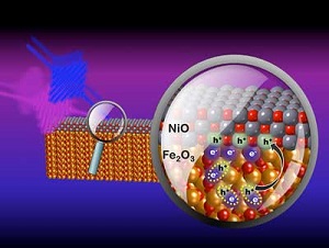
Image Caption: Researchers use extreme ultraviolet pulses (fuchsia line) to determine how visible light (blue line) causes interfacial hole (h+) transfer from iron oxide (Fe2O3) to nickel oxide (NiO), a hole collection layer commonly found in hybrid perovskite solar cells.
Using ultrafast extreme ultraviolet pulses, researchers watched as holes were injected across the interface materials found in hybrid perovskite solar cells. The bursts of extreme ultraviolet light were only femtoseconds in duration. The bursts allowed ultrafast, element-specific measurements.
The experiments revealed what states of the nickel atom are the primary hole-acceptors (Physical Chemistry Chemical Physics, "Identifying the acceptor state in NiO hole collection layers: Direct observation of exciton dissociation and interfacial hole transfer across a Fe2O3/NiO heterojunction").
Learning how charge moves in the material layers of solar cells could reveal missing design parameters. These parameters could let scientists control how charge moves inside solar panels or LEDs, including future designs based on novel materials.
Detailed knowledge of real-time motion of charge in solar-cell materials could help scientists and engineers design better solar cells. Here, scientists need to manage both electrons and the holes that are left behind. Specifically, they need a way to collect and move electron holes, the spots where electrons could be but aren’t.
But there’s a problem. The surface states of oxide materials that facilitate hole transfer are hard to study because it is difficult to probe directly between layers of materials, and the charge dynamics are extremely fast, making it difficult to follow them in real time.
Researchers devised a new way of examining charge transport within layered materials. Their new approach let them watch in real time how holes form and how the resulting electrons move, and they demonstrated the method by characterizing the interface formed with nickel oxide atop iron oxide.
The method employs extreme ultraviolet reflection–absorption spectroscopy using tiny bursts of extreme ultraviolet light only a few femtoseconds in duration. The short bursts allow real-time measurement of electron dynamics, and the burst energy allows element-specific measurements within layered materials.
They found that a transient nickel ion (Ni3+) forms after sunlight excites the underlying iron oxide layer. This tells the researchers how the holes in the nickel oxide work. In addition, the team’s work showed that holes are injected into the nickel oxide layer via a two-step process starting with a fast, field-driven exciton (electron-hole pair) dissociation in the iron layer.
With this research, scientists revealed the chemical nature of the hole acceptor state in nickel oxide. Also, they showed how exciton dissociation and interfacial hole transfer occur at the interface of nickel oxide and iron oxide, a model interface.
Share on:


Testimonial
"The I-Connect007 team is outstanding—kind, responsive, and a true marketing partner. Their design team created fresh, eye-catching ads, and their editorial support polished our content to let our brand shine. Thank you all! "
Sweeney Ng - CEE PCBSuggested Items
SEMI Foundation Honors Applied Materials at SEMICON West with 2025 Excellence in Achievement Award for Talent Development
11/04/2025 | SEMIThe SEMI Foundation announced it recognized Applied Materials, Inc. with the Excellence in Achievement Award at SEMICON West 2025 in Phoenix, Arizona, honoring the company’s outstanding leadership and collaboration in building the next generation of semiconductor talent.
On the Line With… Ultra HDI, Episode 8: “Materials, Up and Coming Capabilities,” Now Available
11/05/2025 | I-Connect007I-Connect007 is excited to announce the release of the eighth episode of its 12-part podcast series, On the Line With… American Standard Circuits: Ultra HDI. In this episode, “Materials, Up and Coming Capabilities,” host Nolan Johnson sits down with resident expert John Johnson, Director of Quality and Advanced Technology at American Standard Circuits, to discuss how material selection influences the Ultra HDI (UHDI) manufacturing process.
New Podcast Episode: “Bonding Innovation: How Adhesives and Coatings Are Powering the Next Generation of Electronics”
11/05/2025 | I-Connect007I-Connect007 has released of a new episode in its Voices of the Industry podcast series, titled “Bonding Innovation: How Adhesives and Coatings Are Powering the Next Generation of Electronics.” Hosted by Nolan Johnson, this insightful discussion dives deep into the evolving world of adhesives and coatings—materials that are redefining performance, reliability, and design in modern electronics manufacturing. Dymax's Doug Katze, a leading expert in adhesive technologies, delivers what can only be described as a master class on how these critical materials are adapting to meet rapidly changing market demands.
Sealed for Survival: Potting Electronics for the Toughest Environments
10/29/2025 | Beth Massey, MacDermid Alpha Electronics SolutionsElectronics deployed in harsh conditions face relentless threats from vibration, impact, chemical contaminants, airborne pollutants, and moisture, conditions that can quickly lead to failure without robust protection. Potting, the process of encapsulating electronics in a protective polymer, is a widely used strategy to safeguard devices from both environmental and mechanical hazards.
Driving Innovation: Mechanical and Optical Processes During Rigid-flex Production
10/28/2025 | Kurt Palmer -- Column: Driving InnovationRigid-flex printed circuit boards are a highly effective solution for placing complex circuitry in tight, three-dimensional spaces. They are now indispensable across a range of industries, from medical devices and aerospace to advanced consumer electronics, helping designers make the most efficient use of available space. However, their unique construction—combining rigid and flexible materials—presents a fundamental challenge for PCB manufacturers.