


 Driving Innovation: Mechanical and Optical Processes During Rigid-flex Production
 It’s Only Common Sense: Your Biggest Competitor Is Complacency
 The Chemical Connection: Onshoring PCB Production—Daunting but Certainly Possible


Taking Diamond Qubits for a Spin
February 13, 2019 | U.S. Department of EnergyEstimated reading time: 2 minutes
Scientists use implanted silicon ions and electricity to increase the spin time of quantum bits, moving closer to the tech needed for quantum networks.
By implanting silicon ions in diamond with extreme precision and then controlling the strain on the crystal structure, scientists showed that they could significantly increase the spin lifetimes of solid-state quantum bits. This is of fundamental importance to quantum mechanics and quantum computing.
Quantum networks could change how we produce and send data. Creating such networks requires generating single phonons—the vibrational motion that characterizes single atoms and nonclassical mechanical states. This work opens the door to achieving a long sought-after goal: deterministically producing phonons. These phonons could be used to interface with other quantum systems such as superconducting qubits. The strain engineering approach developed in this research can also be applied to other quantum emitters and be used to generate scalable quantum networks.
Solid-state quantum bits, or qubits, offer scalability in a quantum network. Such networks could change how computations are done and how data is sent. However, the uncontrolled interaction of a quantum system with its environment can cause the quantum states to collapse, a.k.a. quantum decoherence. While there are a range of techniques available to reduce environmental effects, overcoming thermal decoherence is more challenging. Typically, the only effective strategy is to maintain the quantum system at extremely low temperatures. In Nature Communications, a team shows a different approach to solving this problem. They started with the negatively charged silicon-vacancy center in a diamond, an emerging building block for photonic quantum networks.
Scientists created these silicon-vacancy centers at the Center for Integrated Nanotechnologies using a focused ion beam to precisely implant silicon ions in an array on a diamond substrate. Normally this type of device would be subject to thermal decoherence unless the quantum system is operated at ultracold temperatures. Instead of lowering the temperature, the team took advantage of the fact that the electron-phonon coupling, which is the cause of the thermal decoherence, arises from a high susceptibility of the electronic orbitals to lattice strain.
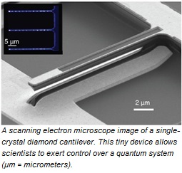
They devised a way to increase the strain. They achieved this with a nano-electro-mechanical system device—a single-crystal diamond cantilever with metal electrodes patterned above and below it. An opening in the top electrode allows optical access to the silicon-vacancy qubits. A direct current voltage applied across the electrodes deflects the cantilever downwards and generates controllable static strain. Through strain control, the team reduced the electron-phonon coupling and demonstrated six-fold improvement in the spin coherence time.
Share on:


Testimonial
"Our marketing partnership with I-Connect007 is already delivering. Just a day after our press release went live, we received a direct inquiry about our updated products!"
Rachael Temple - AlltematedSuggested Items
OSI Systems Reports Fiscal Q1 2026 Financial Results
10/31/2025 | BUSINESS WIREOSI Systems, Inc. announced its financial results for the first quarter of fiscal 2026.
Aircraft Wire and Cable Market to surpass USD 3.2 Billion by 2034
10/30/2025 | Global Market Insights Inc.The global aircraft wire and cable market was valued at USD 1.8 billion in 2024 and is estimated to grow at a CAGR of 5.9% to reach USD 3.2 billion by 2034, according to recent report by Global Market Insights Inc.
David Schild Addresses Printed Circuit Board Issues as a Panelist at AUVSI
10/30/2025 | PCBAAOn October 28, Printed Circuit Board Association of America executive director David Schild appeared on a panel at the Association for Uncrewed Vehicle Systems International (AUVSI) conference on the topic of “First Supply Chains: Strengthening the Industrial Base for Autonomy.” PCBAA sponsored the event and Schild shared his views on issues facing the American microelectronics industry.
Real Time with... SMTAI 2025: Koh Young's Innovations in SMT Inspection Technology
10/30/2025 | Real Time with...SMTAIJoel Scutchfield discusses his background as well as Koh Young's advancements in inspection technology. The conversation covers various inspection systems, including the flagship Zenith 2 system and recent software upgrades.
BAE Contract Agreed with the Republic of Türkiye for Typhoon Aircraft
10/28/2025 | BAE SystemsThe UK Government has announced a c.£5.4 billion agreement with the Republic of Türkiye for the purchase of 20 Typhoon aircraft and an associated weapons and integration package, sustaining more than 20,000 highly skilled jobs across the UK supply chain.