


 Driving Innovation: Mechanical and Optical Processes During Rigid-flex Production
 It’s Only Common Sense: Your Biggest Competitor Is Complacency
 The Chemical Connection: Onshoring PCB Production—Daunting but Certainly Possible


Customized Mix of Materials for 3D Micro- and Nanostructures
February 14, 2019 | KITEstimated reading time: 2 minutes
Three-dimensional structures on the micrometer and nanometer scales have a great potential for many applications. An efficient and precise process to print such structures from different materials is now presented by researchers of Karlsruhe Institute of Technology (KIT) and Carl Zeiss AG in Science Advances: they integrated a microfluidic chamber into a 3D laser lithography device. Then, they used this system to produce multi-colored, fluorescent security features to protect banknotes, documents, and branded products against counterfeiting.
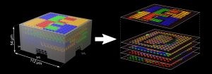
Image Caption: Multi-colored fluorescent security feature in computer design (left) and its layers under the laser scanning microscope (right). (Figure: Frederik Mayer, INT/KIT)
From components for data processing with light to optical microlenses, mechanical metamaterials, or artificial scaffolds for cell cultures to security features of banknotes or branded products, printed three-dimensional micro- and nanostructures have a large range of applications. 3D laser lithography has become an established, reliable, and versatile process for their production. A laser beam is passed through a liquid photoresist in a computer-controlled way and the material is exposed and hardened at the focal point of the laser beam only. This gives rise to highly precise filigree structures for many applications, including optics and photonics, materials sciences, biotechnology or security technology. Nearly all of the micro- and nanostructures produced by 3D laser lithography so far consist of a single material. But they might also be manufactured from several materials by successive application and hardening of different photoresists, with the unexposed resist being washed out in a subsequent developing bath. Such a process, however, is very time-consuming and complicated and its precision decreases with an increasing number of materials and repetitions.
Within the Cluster of Excellence “3D Matter Made to Order,” scientists of KIT’s Institutes of Nanotechnology (INT), of Applied Physics (APH), for Chemical Technology and Polymer Chemistry (ITCP), and of the School of Chemistry of Queensland University of Technology (QUT) in Brisbane/Australia, together with researchers of Carl Zeiss AG, have now developed a new system for the efficient and precise production of printed micro- and nanostructures from several materials. They integrated a microfluidic chamber for the fluids on smallest space directly into a 3D laser lithography device.
In their publication “Multimaterial 3D Laser Microprinting Using an Integrated Microfluidic System” in Science Advances, the researchers report that they used the integrated system to produce three-dimensional microstructured security features from seven different fluids: a non-fluorescent photoresist as backbone, two photoresists with different fluorescent quantum points, two photoresists with different fluorescent dyes, and two developer fluids. Such security features may protect banknotes, documents, and branded products against counterfeiting. A security feature consists of a three-dimensional lattice enclosed by retaining walls and fluorescent markers in different colors.
For their system, the scientists used a 3D laser lithography device developed and commercialized by Nanoscribe GmbH, a spinoff of KIT, and integrated it into a self-developed microfluidic chamber. It is provided with a cover glass of ten millimeters in diameter onto which the 3D structures can be printed. The chamber is connected to an electronic pressure control, up to ten containers for the different photoresists and developers, and a star-shaped selection valve. The fluid selected is passed to a specimen holder via an overpressure valve. Finally, it flows into a waste container. “All steps for producing three-dimensional micro- and nanostructures from several materials can be integrated into one system,” says Professor Martin Wegener, who heads the working group at APH. “This system paves the way towards multi-material additive manufacture on the micro- and nanoscale.”
Share on:


Testimonial
"We’re proud to call I-Connect007 a trusted partner. Their innovative approach and industry insight made our podcast collaboration a success by connecting us with the right audience and delivering real results."
Julia McCaffrey - NCAB GroupSuggested Items
OSI Systems Reports Fiscal Q1 2026 Financial Results
10/31/2025 | BUSINESS WIREOSI Systems, Inc. announced its financial results for the first quarter of fiscal 2026.
Aircraft Wire and Cable Market to surpass USD 3.2 Billion by 2034
10/30/2025 | Global Market Insights Inc.The global aircraft wire and cable market was valued at USD 1.8 billion in 2024 and is estimated to grow at a CAGR of 5.9% to reach USD 3.2 billion by 2034, according to recent report by Global Market Insights Inc.
David Schild Addresses Printed Circuit Board Issues as a Panelist at AUVSI
10/30/2025 | PCBAAOn October 28, Printed Circuit Board Association of America executive director David Schild appeared on a panel at the Association for Uncrewed Vehicle Systems International (AUVSI) conference on the topic of “First Supply Chains: Strengthening the Industrial Base for Autonomy.” PCBAA sponsored the event and Schild shared his views on issues facing the American microelectronics industry.
Real Time with... SMTAI 2025: Koh Young's Innovations in SMT Inspection Technology
10/30/2025 | Real Time with...SMTAIJoel Scutchfield discusses his background as well as Koh Young's advancements in inspection technology. The conversation covers various inspection systems, including the flagship Zenith 2 system and recent software upgrades.
BAE Contract Agreed with the Republic of Türkiye for Typhoon Aircraft
10/28/2025 | BAE SystemsThe UK Government has announced a c.£5.4 billion agreement with the Republic of Türkiye for the purchase of 20 Typhoon aircraft and an associated weapons and integration package, sustaining more than 20,000 highly skilled jobs across the UK supply chain.