


 Driving Innovation: Mechanical and Optical Processes During Rigid-flex Production
 It’s Only Common Sense: Your Biggest Competitor Is Complacency
 The Chemical Connection: Onshoring PCB Production—Daunting but Certainly Possible


Collaboration Sparks Sustainable Electronics Manufacturing Breakthrough
February 14, 2019 | Simon Fraser UniversityEstimated reading time: 2 minutes
Simon Fraser University and Swiss researchers are developing an eco-friendly, 3D printable solution for producing wireless Internet-of-Things (IoT) sensors that can be used and disposed of without contaminating the environment.
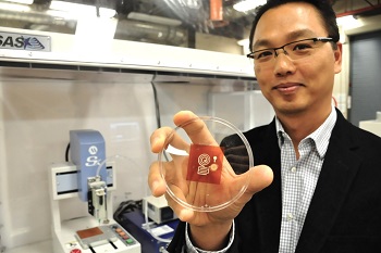
Image Caption: SFU Mechatronic Systems Engineering professor Woo Soo Kim is collaborating with Swiss researchers to develop an eco-friendly 3D printable solution for producing wireless Internet-of-Things sensors. The research team is using a wood-derived cellulose material to replace the plastics and polymeric materials currently used in electronics.
SFU professor Woo Soo Kim is leading the research team's discovery involving the use of a wood-derived cellulose material to replace the plastics and polymeric materials currently used in electronics.
Additionally, 3D printing can give flexibility to add or embed functions onto 3D shapes or textiles, creating greater functionality.
“Our eco-friendly 3D printed cellulose sensors can wirelessly transmit data during their life, and then can be disposed without concern of environmental contamination,” says Kim, a professor in the School of Mechatronic Systems Engineering. The SFU research is being carried out at PowerTech Labs in Surrey, which houses several state-of-the-art 3D printers used to advance the research.
“This development will help to advance green electronics. For example, the waste from printed circuit boards is a hazardous source of contamination to the environment. If we are able to change the plastics in PCB to cellulose composite materials, recycling of metal components on the board could be collected in a much easier way.”
Kim’s research program spans two international collaborative projects, including the latest focusing on the eco-friendly cellulose material-based chemical sensors with collaborators from the Swiss Federal Laboratories for Materials Science.
He is also collaborating with a team of South Korean researchers from the Daegu Gyeongbuk Institute of Science and Technology’s (DGIST)’s department of Robotics Engineering, and PROTEM Co Inc, a technology-based company, for the development of printable conductive ink materials.
In this second project, researchers have developed a new breakthrough in the embossing process technology, one that can freely imprint fine circuit patterns on flexible polymer substrate, a necessary component of electronic products.
Embossing technology is applied for the mass imprinting of precise patterns at a low unit cost. However, Kim says it can only imprint circuit patterns that are imprinted beforehand on the pattern stamp, and the entire, costly stamp must be changed to put in different patterns.
The team succeeded in developing a precise location control system that can imprint patterns directly resulting in a new process technology. The result will have widespread implications for use in semiconductor processes, wearable devices and the display industry.
Earlier this year Kim was selected as a Brain Pool Fellow by the National Research Foundation (NRF) of Korea.
An expert in 3D printed electronics who heads SFU’s Additive Manufacturing Laboratory, he spent six months collaborating with researchers at Seoul National University to advance fabrication of thin film transistors using 3D printing technology.
Share on:


Testimonial
"Our marketing partnership with I-Connect007 is already delivering. Just a day after our press release went live, we received a direct inquiry about our updated products!"
Rachael Temple - AlltematedSuggested Items
KYZEN Honored with 2025 Step-by-Step Excellence Award for Its Innovative ANALYST² Process Control System
10/31/2025 | KYZEN'KYZEN, the global leader in innovative environmentally responsible cleaning chemistries, is proud to announce that its ANALYST² Process Control System has won a 2025 Step-by-Step Excellence Award (SbSEA).
LPKF Delivers Key Strategic Technology to Fraunhofer's Glass Panel Technology Group
10/29/2025 | LPKFLPKF Laser & Electronics SE is one of the initiators of the Glass Panel Technology Group (GPTG), a consortium encompassing the entire process chain for advanced semiconductor packaging with glass substrates.
On the Line With… Ultra HDI Podcast—Episode 7: “Solder Mask: Beyond the Traces,” Now Available
10/29/2025 | I-Connect007I-Connect007 is excited to announce the release of the seventh episode of its 12-part podcast series, On the Line With… American Standard Circuits: Ultra HDI. In this episode, “Solder Mask: Beyond the Traces,” host Nolan Johnson sits down with John Johnson, Director of Quality and Advanced Technology at American Standard Circuits, to explore the essential role that solder mask plays in the Ultra HDI (UHDI) manufacturing process.
Nvidia’s Blackwell Chips Made in Arizona Still Head to Taiwan for Final Assembly
10/27/2025 | I-Connect007 Editorial TeamNvidia has begun production of its next-generation Blackwell GPUs in the United States, but the company still depends heavily on Taiwan to complete the process, The Register reported.
American Standard Circuits Launches 50th 77-Second Webinar
10/27/2025 | American Standard CircuitsAnaya Vardya, President and CEO of American Standard Circuits/ASC Sunstone Circuits is pleased to announce that they have recently unveiled their 50th 77-second webinar.