


 Driving Innovation: Mechanical and Optical Processes During Rigid-flex Production
 It’s Only Common Sense: Your Biggest Competitor Is Complacency
 The Chemical Connection: Onshoring PCB Production—Daunting but Certainly Possible


Graphene and Boron Nitride ‘Sandwich’ Key to New Electronics
February 19, 2019 | Graphene FlagshipEstimated reading time: 3 minutes
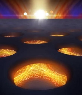
Since its inception, scientists have tried to exploit graphene to produce nano-sized electronics. However, since graphene is only an atom thick, all atoms are exposed to the outside world, and even small amounts of defects and impurities impede its properties. Now, Graphene Flagship researchers at DTU, Denmark solved this problem by protecting graphene with insulating layers of hexagonal boron nitride, another two-dimensional material with insulating properties.
Peter Bøggild, researcher at Graphene Flagship partner DTU and coauthor of the paper, explains that although "graphene is a fantastic material that could play a crucial role in making new nano-sized electronics, it is still extremely difficult to control its electrical properties." Since 2010, scientists at DTU have tried to tailor the electrical properties of graphene, by making a very fine pattern of holes, so that channels through which an electric power can flow freely are formed.
"Creating nanostructured graphene turned out to be amazingly difficult, since even small errors wash out all the properties we designed it to have," comments Bøggild.
Now, researchers from Graphene Flagship partner DTU made a leap forward. Bjarke Jessen and Lene Gammelgaard encapsulated graphene with another 2D material, hexagonal boron nitride, which is very similar to graphene, but electrically insulating. Then, using nanolithography, they carefully drilled nanoscopic holes in graphene through the protective layer of boron nitride. The holes have a diameter of approximately 20 nanometers, and are separated from each other with just 12 nanometers. This great precision makes possible to send an electrical current through the graphene that is 100-1000 times higher than typical numbers for lithographically carved nanographene.
"When you make patterns in a material like graphene, you do so in order to change its properties. However, what we have seen throughout the years is that when we shape graphene on this fine scale, it does not behave like graphene anymore - there is too much disorder,’ explains Bøggild. ‘Many scientists have abandoned nanolithography in graphene on this scale, but now we have figured out how it can be done - you could say that the curse is lifted," he adds.
"We have shown that we can control graphene’s band structure and that deterministic design of nanoelectronics is realistic. Looking solely at electronics, this means that we can make insulators, transistors, conductors and perhaps even superconductors, as our nanolithography can preserve the subtle inter-layer physics that was recently shown to lead to superconductivity in double-layer graphene. However, it goes way beyond that. When we control the band structure, we have access to all of graphene’s properties. In other words, we could sit in front of the computer and dream up other applications - and then go to the laboratory and make them happen," says Bøggild. ‘There are plenty of practical challenges, but the fact that we can tailor electronic properties of graphene is a big step towards creating new electronics with extremely small dimensions,’ he concludes.
Daniel Neumaier, Graphene Flagship Division Leader for Electronics and Photonics Integration says: ‘Controlling the electronic properties of graphene by nano-pattering offers an additional degree of freedom for the design of electronic and photonic devices, which was so far not accessible. The researchers from Graphene Flagship partner DTU and their co-workers now discovered a unique way for nano-patterning of graphene without seeing the limitations of patterning introduced defects. This was the key enabling step for using the nano-patterning induced electronic properties of graphene in real device and we are expecting significant advances especially for nano-electronics and photonics based on these results.’
Andrea C. Ferrari, Science and Technology Officer of the Graphene Flagship and Chair of its Management Panel added how "patterning of graphene to create nano-electronic devices was one of the first approaches attempted to exploit this unique material into devices. However, after an initial flurry of publications, the amount of damage produced was so much that this line of research was almost entirely abandoned. The work presented here shows how the long term nature of the Flagship allows scientists to pursue and solve even apparently intractable problems. This will rejuvenate the interest in graphene nanoelectronics, and could lead to a variety of useful devices, previously hampered by defects."
Share on:


Testimonial
"The I-Connect007 team is outstanding—kind, responsive, and a true marketing partner. Their design team created fresh, eye-catching ads, and their editorial support polished our content to let our brand shine. Thank you all! "
Sweeney Ng - CEE PCBSuggested Items
I-Connect007 Editor’s Choice: Five Must-Reads for the Week
10/31/2025 | Nolan Johnson, I-Connect007Last week, the IMPACT conference took place in Taipei, bringing together advanced packaging experts from around the globe to share their knowledge. We’ll be bringing you post-conference coverage over the next few weeks, so look for that in our newsletters, and in the Advanced Electronic Packaging Digest. Other news seemed to have the U.S. at the center of the global discussions. My picks start in Phoenix, where TSMC, NVIDIA, and Amkor are all scrambling to establish new capabilities. There’s nothing like a strong demand signal to cause build-out, and AI chips are doing exactly that.
NEDME 2025 Draws Strong Northwest Crowd, Builds on Tradition of Regional Collaboration
10/31/2025 | NEDMEThe NW Electronics Design & Manufacturing Expo (NEDME) 2025 once again brought together the Pacific Northwest community for a full day of learning, networking, and industry connections.
The Training Connection Continues to Grow with Addition of Veteran IPC Trainer Bill Graver
10/30/2025 | The Training Connection LLCThe Training Connection, LLC (TTC-LLC), a premier provider of test engineering and development training, is proud to announce the addition of Bill Graver to its growing team of industry experts. A respected professional with more than 35 years in electronics manufacturing, Bill joins as an IPC Master Trainer, bringing a wealth of hands-on experience in PCB testing, failure analysis, and process improvement.
I-Connect007 Welcomes New Columnist: Leo Lambert, EPTAC
10/30/2025 | I-Connect007I-Connect007 is excited to announce a column by Leo Lambert, an industry veteran with 40 years of experience, an award winner, and technical director at EPTAC. This column, Learning With Leo, will explore the evolution and related challenges of electronics product assembly, especially as it relates to training.
Cicor to Acquire UK-Based TT Electronics with Board Support
10/30/2025 | Cicor Technologies Ltd.Cicor is a globally active provider of full-cycle electronic solutions (EMS) for the healthcare technology, industrial, and aerospace & defense sectors. TT is a UK-based, London Stock Exchange-listed global provider of engineered electronics for performance critical applications.