


 Global PCB Connections: Rigid-flex and Flexible PCBs—The Backbone of Modern Electronics
 Flexible Thinking: The Key to a Successful Flex Circuit Design Transfer
 Happy’s Tech Talk #29: Bend-to-Install Semi-flex FR-4


A Flexible Future
February 20, 2019 | UNSW SydneyEstimated reading time: 2 minutes
Thin, flexible panels that will revolutionise how we use solar energy are on the drawing board at UNSW. Imagine a future in which thin, flexible solar panels cover the surfaces of cars and buildings, powering their activities.
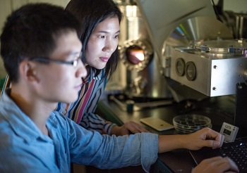
Xiaojing Hao, associate professor and Scientia fellow in the School of Photovoltaic and Renewable Energy Engineering, and her team, are building such cells made of kesterite photovoltaics.
Containing copper, zinc, tin and sulphur, they are cheaper to make and more environmentally friendly than other thin-film varieties on the market, some of which contain toxic materials, such as cadmium, or rare elements, such as indium and tellurium.
There are significant industrial applications for flexible, thin photovoltaic cells. But a key challenge has been their limited capacity to generate energy with a comparable efficiency and cost to that of conventional silicon solar panels.
In 2017, A/Prof Hao’s team built a kesterite photovoltaic cell that attained 11% efficiency. This set a world record—a fourth for the team—and was the first time that the 10% efficiency threshold was broken for this type of cell. This work was published in the Nature Energy journal in 2018.
“For each efficiency change, we need a step-change technology to make it happen,” says A/Prof Hao. She hopes to improve the efficiency of kesterite photovoltaic cells to close to 20% in the next five years.
To do this, her team needs to work out how to prevent the common defects in the lattice of the kesterite material. The reasons for these defects are not yet well understood. However, once corrected, the electrical quality of the material—the main barrier to efficiency—will improve.
Exciting findings from 2018 point to some new directions to control the defects and improve the performance of kesterite cells. The plan is to apply for Australian Research Council funding to delve deeper and publish some of these results in 2019.
Dr Xiaojing Hao of UNSW's Australian Centre for Advanced Photovoltaics holding the new CZTS solar cells.
In 2017, A/Prof Hao was one of 18 young scientists selected from more than 1000 applicants to take up one of UNSW’s inaugural Scientia fellowships. Last year, she won two prestigious prizes: the $5000 Premier’s Prize for Energy Innovation from the state of New South Wales and the $3000 UNSW Engineering Faculty Dean’s Award for Excellence in Research. A/Prof Hao’s enthusiasm for discovery is given free rein at UNSW.
“I love to explore the unknowns and deal with challenges. Achieving research progress, particularly through challenging work, brings me deep fulfilment.”
Share on:


Testimonial
"Advertising in PCB007 Magazine has been a great way to showcase our bare board testers to the right audience. The I-Connect007 team makes the process smooth and professional. We’re proud to be featured in such a trusted publication."
Klaus Koziol - atgSuggested Items
Closing the Loop on PCB Etching Waste
09/09/2025 | Shawn Stone, IECAs the PCB industry continues its push toward greener, more cost-efficient operations, Sigma Engineering’s Mecer System offers a comprehensive solution to two of the industry’s most persistent pain points: etchant consumption and rinse water waste. Designed as a modular, fully automated platform, the Mecer System regenerates spent copper etchants—both alkaline and acidic—and simultaneously recycles rinse water, transforming a traditionally linear chemical process into a closed-loop system.
Driving Innovation: Depth Routing Processes—Achieving Unparalleled Precision in Complex PCBs
09/08/2025 | Kurt Palmer -- Column: Driving InnovationIn PCB manufacturing, the demand for increasingly complex and miniaturized designs continually pushes the boundaries of traditional fabrication methods, including depth routing. Success in these applications demands not only on robust machinery but also sophisticated control functions. PCB manufacturers rely on advanced machine features and process methodologies to meet their precise depth routing goals. Here, I’ll explore some crucial functions that empower manufacturers to master complex depth routing challenges.
Trouble in Your Tank: Minimizing Small-via Defects for High-reliability PCBs
08/27/2025 | Michael Carano -- Column: Trouble in Your TankTo quote the comedian Stephen Wright, “If at first you don’t succeed, then skydiving is not for you.” That can be the battle cry when you find that only small-diameter vias are exhibiting voids. Why are small holes more prone to voids than larger vias when processed through electroless copper? There are several reasons.
The Government Circuit: Navigating New Trade Headwinds and New Partnerships
08/25/2025 | Chris Mitchell -- Column: The Government CircuitAs global trade winds continue to howl, the electronics manufacturing industry finds itself at a critical juncture. After months of warnings, the U.S. Government has implemented a broad array of tariff increases, with fresh duties hitting copper-based products, semiconductors, and imports from many nations. On the positive side, tentative trade agreements with Europe, China, Japan, and other nations are providing at least some clarity and counterbalance.
How Good Design Enables Sustainable PCBs
08/21/2025 | Gerry Partida, Summit InterconnectSustainability has become a key focus for PCB companies seeking to reduce waste, conserve energy, and optimize resources. While many discussions on sustainability center around materials or energy-efficient processes, PCB design is an often overlooked factor that lies at the heart of manufacturing. Good design practices, especially those based on established IPC standards, play a central role in enabling sustainable PCB production. By ensuring designs are manufacturable and reliable, engineers can significantly reduce the environmental impact of their products.