


 Driving Innovation: Mechanical and Optical Processes During Rigid-flex Production
 It’s Only Common Sense: Your Biggest Competitor Is Complacency
 The Chemical Connection: Onshoring PCB Production—Daunting but Certainly Possible


In-Memory Computing Using Photonic Memory Devices
February 20, 2019 | IBMEstimated reading time: 3 minutes
Could light be the answer to the future of more energy-efficient and faster computing?
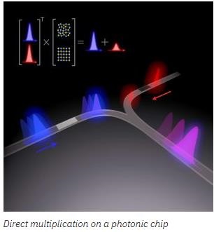
Today, our collaborative team of scientists led by Oxford and IBM Research-Zurich, with colleagues at Exeter and Munster, published a new research paper that points to its potential. Together we have developed an all-optical approach to developing direct in-memory multiplication on an integrated photonic device based on non-volatile multilevel phase-change memories. Electronic phase change memory (PCM) is an emerging non-volatile memory technology that could play a significant role in future computing systems. Using integrated photonic technology will potentially offer attractive solutions for using light to carry out computational tasks on a chip in future.
This concept of implementing in-memory computing on an integrated photonic chip has the ability to further transform the computing landscape, especially since speeds and bandwidths working directly on an optical domain are increased. In a nutshell, this means faster detection, expanded operations, and decreased energy consumption.
Overcoming the Challenges
In recent years, integrated photonic memories have been widely investigated. However, researchers have not been able to overcome the challenges pertaining to energy switching, speed, and detection latency that arise when carrying out computational tasks on the same device simultaneously implementing memory function. Our research team set out to address these very challenges—a task we accomplished with success.
In our work, we demonstrate the first instance of a photonic computational memory for direct scalar multiplication of two numbers, using a single integrated photonic memory change cell. Our device relies on the distinct interaction of two pulses, both of which represent a number to be multiplied. One pulsation gives energy above the switching threshold to induce structural changes in the material, and the other below in an integrated photonic waveguide. Going a step further, we then used non-volatile photonic elements based on the phase change material (Ge2Sb2Te5) to achieve direct scalar and matrix-vector multiplication.
Photonic Advantages
In-memory computing already breaks the processor-memory dichotomy allowing processing to take place in the memory elements. An electrical implementation of such a system is able to carry out complex tasks such as scalar multiplications, correlation detection, and compressed sensing recovery. Moving from an electrical to an optical domain has even more advantages. In photonic implementations of in-memory computing on an integrated photonic chip, not only do speed and bandwidths increase, detection latency also improves as processing takes place directly on an optical domain using light.
Essentially, our findings confirm the potential of phase-change materials in photonic hardware. We prove that it is possible to combine integrated optics with collocated data storage and processing to enable all-photonic in-memory computations. And by optimizing the ratio of memory cell size to pulse width in our integrated photonic device, we were able to significantly decrease energy consumption. This enables pulse-shaping routes and optimizes the device design to make further gains in energy and speed
The Big Picture
Our all-optical approach is not only unique, it is also easy to fabricate and operate. Moreover, it sets the stage for developing fully photonic operating computers. In the grand schemes of things, our work represents a key milestone for optical processing in memory. What’s more, matrix-vector multiplication operations using multiple phase memory cells have the potential to underpin key processing operations in computational areas such as big data analytics and artificial intelligence. But the list does not stop there. Such an architecture could efficiently solve systems of linear equations and advance various other emerging computational areas, including machine learning and deep learning. The next step is to figure out how to neatly scale up matrix sizes on photonic chips — a challenge we are working on right now.
Share on:


Testimonial
"We’re proud to call I-Connect007 a trusted partner. Their innovative approach and industry insight made our podcast collaboration a success by connecting us with the right audience and delivering real results."
Julia McCaffrey - NCAB GroupSuggested Items
Yonsei University Develops a New Era of High-Voltage Solid-State Batteries
10/31/2025 | PRNewswireResearchers at Yonsei University developed a fluoride-based solid electrolyte (LiCl–4Li₂TiF₆) that enables all-solid-state batteries to operate safely beyond 5 volts, overcoming a major voltage stability barrier.
Argonne Expands Nation’s AI Infrastructure With Powerful New Supercomputers and Public-Private Partnerships
10/29/2025 | BUSINESS WIREThe U.S. Department of Energy (DOE), Argonne National Laboratory, NVIDIA and Oracle announced a landmark public-private partnership to deliver the DOE’s largest AI supercomputer and accelerate scientific discovery.
Singapore’s Largest Industrial District Cooling System Begins Operations to Support STMicroelectronics’ Decarbonization Strategy
10/27/2025 | STMicroelectronicsSTMicroelectronics, a global semiconductor leader serving customers across the spectrum of electronics applications, and SP Group (SP), a leading utilities group in the Asia Pacific and Singapore’s national grid operator, have commenced operations for Singapore’s largest industrial district cooling system at STMicroelectronics’ (ST) Ang Mo Kio TechnoPark.
SemiQon's Cryogenic Chip Technology for Quantum Computing and Space Applications Receives Award from EARTO
10/17/2025 | PRNewswireEARTO, the organisation of the European Research and Technology Organisations, awarded SemiQon and VTT first prize in the "Impact Expected" category on 14 October 2025 in Brussels for a pioneering cryogenic CMOS (complementary metal-oxide semiconductor) chip innovation.
Optimum Energy Powers Up Partnership with Conference USA
10/17/2025 | BUSINESS WIREOptimum Energy, a leading energy as a service provider for higher education, announced it will serve as a premier corporate sponsor for Conference USA (CUSA).