


 Driving Innovation: Mechanical and Optical Processes During Rigid-flex Production
 It’s Only Common Sense: Your Biggest Competitor Is Complacency
 The Chemical Connection: Onshoring PCB Production—Daunting but Certainly Possible


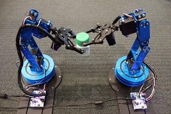
Robots Track Moving Objects With Unprecedented Precision
February 20, 2019 | MITEstimated reading time: 5 minutes
System uses RFID tags to home in on targets; could benefit robotic manufacturing, collaborative drones, and other applications.
A novel system developed at MIT uses RFID tags to help robots home in on moving objects with unprecedented speed and accuracy. The system could enable greater collaboration and precision by robots working on packaging and assembly, and by swarms of drones carrying out search-and-rescue missions.
In a paper being presented next week at the USENIX Symposium on Networked Systems Design and Implementation, the researchers show that robots using the system can locate tagged objects within 7.5 milliseconds, on average, and with an error of less than a centimeter.
In the system, called TurboTrack, an RFID (radio-frequency identification) tag can be applied to any object. A reader sends a wireless signal that reflects off the RFID tag and other nearby objects, and rebounds to the reader. An algorithm sifts through all the reflected signals to find the RFID tag’s response. Final computations then leverage the RFID tag’s movement — even though this usually decreases precision — to improve its localization accuracy.
The researchers say the system could replace computer vision for some robotic tasks. As with its human counterpart, computer vision is limited by what it can see, and it can fail to notice objects in cluttered environments. Radio frequency signals have no such restrictions: They can identify targets without visualization, within clutter and through walls.
To validate the system, the researchers attached one RFID tag to a cap and another to a bottle. A robotic arm located the cap and placed it onto the bottle, held by another robotic arm. In another demonstration, the researchers tracked RFID-equipped nanodrones during docking, maneuvering, and flying. In both tasks, the system was as accurate and fast as traditional computer-vision systems, while working in scenarios where computer vision fails, the researchers report.
“If you use RF signals for tasks typically done using computer vision, not only do you enable robots to do human things, but you can also enable them to do superhuman things,” says Fadel Adib, an assistant professor and principal investigator in the MIT Media Lab, and founding director of the Signal Kinetics Research Group. “And you can do it in a scalable way, because these RFID tags are only 3 cents each.”
In manufacturing, the system could enable robot arms to be more precise and versatile in, say, picking up, assembling, and packaging items along an assembly line. Another promising application is using handheld “nanodrones” for search and rescue missions. Nanodrones currently use computer vision and methods to stitch together captured images for localization purposes. These drones often get confused in chaotic areas, lose each other behind walls, and can’t uniquely identify each other. This all limits their ability to, say, spread out over an area and collaborate to search for a missing person. Using the researchers’ system, nanodrones in swarms could better locate each other, for greater control and collaboration.
“You could enable a swarm of nanodrones to form in certain ways, fly into cluttered environments, and even environments hidden from sight, with great precision,” says first author Zhihong Luo, a graduate student in the Signal Kinetics Research Group.
The other Media Lab co-authors on the paper are visiting student Qiping Zhang, postdoc Yunfei Ma, and Research Assistant Manish Singh.
Page 1 of 2
Share on:


Testimonial
"The I-Connect007 team is outstanding—kind, responsive, and a true marketing partner. Their design team created fresh, eye-catching ads, and their editorial support polished our content to let our brand shine. Thank you all! "
Sweeney Ng - CEE PCBSuggested Items
Aircraft Wire and Cable Market to surpass USD 3.2 Billion by 2034
10/30/2025 | Global Market Insights Inc.The global aircraft wire and cable market was valued at USD 1.8 billion in 2024 and is estimated to grow at a CAGR of 5.9% to reach USD 3.2 billion by 2034, according to recent report by Global Market Insights Inc.
David Schild Addresses Printed Circuit Board Issues as a Panelist at AUVSI
10/30/2025 | PCBAAOn October 28, Printed Circuit Board Association of America executive director David Schild appeared on a panel at the Association for Uncrewed Vehicle Systems International (AUVSI) conference on the topic of “First Supply Chains: Strengthening the Industrial Base for Autonomy.” PCBAA sponsored the event and Schild shared his views on issues facing the American microelectronics industry.
Real Time with... SMTAI 2025: Koh Young's Innovations in SMT Inspection Technology
10/30/2025 | Real Time with...SMTAIJoel Scutchfield discusses his background as well as Koh Young's advancements in inspection technology. The conversation covers various inspection systems, including the flagship Zenith 2 system and recent software upgrades.
BAE Contract Agreed with the Republic of Türkiye for Typhoon Aircraft
10/28/2025 | BAE SystemsThe UK Government has announced a c.£5.4 billion agreement with the Republic of Türkiye for the purchase of 20 Typhoon aircraft and an associated weapons and integration package, sustaining more than 20,000 highly skilled jobs across the UK supply chain.
Singapore’s Largest Industrial District Cooling System Begins Operations to Support STMicroelectronics’ Decarbonization Strategy
10/27/2025 | STMicroelectronicsSTMicroelectronics, a global semiconductor leader serving customers across the spectrum of electronics applications, and SP Group (SP), a leading utilities group in the Asia Pacific and Singapore’s national grid operator, have commenced operations for Singapore’s largest industrial district cooling system at STMicroelectronics’ (ST) Ang Mo Kio TechnoPark.