


 Driving Innovation: Mechanical and Optical Processes During Rigid-flex Production
 It’s Only Common Sense: Your Biggest Competitor Is Complacency
 The Chemical Connection: Onshoring PCB Production—Daunting but Certainly Possible


Advances in Logic IC Process Technology Move Forward
February 22, 2019 | IC InsightsEstimated reading time: 3 minutes
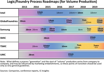
The advancement of the IC industry hinges on the ability of IC manufacturers to continue offering more performance and functionality for the money. As mainstream CMOS processes reach their theoretical, practical, and economic limits, lowering the cost of ICs (on a per-function or per-performance basis) is more critical and challenging than ever. The 500-page, 2019 edition of IC Insights’ McClean Report—A Complete Analysis and Forecast of the Integrated Circuit Industry (released in January 2019) shows that there is more variety than ever among the logic-oriented process technologies that companies offer. The figure lists several of the leading advanced logic technologies that companies are presently using. Derivative versions of each process generation between major nodes have become regular occurrences.
Intel — Its ninth-generation processors unveiled in late 2018 have the code-name “Coffee Lake-S” or, sometimes called “Coffee Lake Refresh.” Intel says these processors are a new generation of products, but they seem to be more of an enhancement of the eighth-generation products. Details are scarce, but these processors appear to be manufactured on an enhanced version of the 14nm++ process, or what might be considered a 14nm+++ process.
Mass production using its 10nm process will ramp in 2019 with the new “Sunny Cove” family of processors that it unveiled in December 2018. It appears that the Sunny Cove architecture has essentially taken the place of the 10nm Cannon Lake architecture that was supposed to be released in 2019. In 2020, a 10nm+ derivative process is expected to go into mass production.
TSMC — TSMC’s 10nm finFET process entered volume production in late 2016 but it has moved quickly from 10nm to 7nm. TSMC believes the 7nm generation will be a long-lived node like 28nm and 16nm.
TSMC’s 5nm process is under development and scheduled to enter risk production in the first half of 2019, with volume production coming in 2020. The process will use EUV, but it will not be the first of TSMC’s processes to take advantage of EUV technology. The first will be an improved version of the company’s 7nm technology. The N7+ process will employ EUV only on critical layers (four layers), while the N5 process will use EUV extensively (up to 14 layers). N7+ is scheduled to enter volume production in the second quarter of 2019.
Samsung — In early 2018, Samsung started mass production of a second-generation 10nm process called 10LPP (low power plus). Later in 2018, Samsung introduced a third-generation 10nm process called 10LPU (low power ultimate) that provided another performance increase. Samsung uses triple patterning lithography at 10nm. Unlike TSMC, Samsung believes its 10nm family of processes (including 8nm derivatives) will have a long lifecycle.
Samsung’s 7nm technology went into risk production in October 2018. The company skipped offering a 7nm process with immersion lithography and decided instead to move directly to a EUV-based 7nm process. The company is using EUV for 8-10 layers at 7nm.
GlobalFoundries — GF views and markets its 22nm FD-SOI process as being complementary to its 14nm finFET technology. The company says the 22FDX platform delivers performance very close to that of finFET, but with manufacturing costs the same as 28nm technology.
In August 2018, GlobalFoundries made a major shift in strategy by announcing it would halt 7nm development because of the enormous expense in ramping production at that technology node and because there were too few foundry customers planning to use the next-generation process. As a result, the company shifted its R&D efforts to further enhance its 14nm and 12nm finFET processes and its fully depleted SOI technologies.
For five decades, there have been amazing improvements in the productivity and performance of integrated circuit technology. While the industry has surmounted many obstacles put in front of it, it seems the barriers keep getting bigger. Despite this, IC designers and manufacturers are developing solutions that seem more revolutionary than evolutionary to increase chip functionality.
Share on:


Testimonial
"The I-Connect007 team is outstanding—kind, responsive, and a true marketing partner. Their design team created fresh, eye-catching ads, and their editorial support polished our content to let our brand shine. Thank you all! "
Sweeney Ng - CEE PCBSuggested Items
Meet the Author Podcast: Martyn Gaudion Unpacks the Secrets of High-Speed PCB Design
07/16/2025 | I-Connect007In this special Meet the Author episode of the On the Line with… podcast, Nolan Johnson sits down with Martyn Gaudion, signal integrity expert, managing director of Polar Instruments, and three-time author in I-Connect007’s popular The Printed Circuit Designer’s Guide to... series.
Intervala Hosts Employee Car and Motorcycle Show, Benefit Nonprofits
08/27/2024 | IntervalaIntervala hosted an employee car and motorcycle show, aptly named the Vala-Cruise and it was a roaring success! Employees had the chance to show off their prized wheels, and it was incredible to see the variety and passion on display.
KIC Honored with IPC Recognition for 25 Years of Membership and Contributions to Electronics Manufacturing Industry
06/24/2024 | KICKIC, a renowned pioneer in thermal process and temperature measurement solutions for electronics manufacturing, is proud to announce that it has been recognized by IPC for 25 years of membership and significant contributions to electronics manufacturing.
Boeing Starliner Spacecraft Completes Successful Crewed Docking with International Space Station
06/07/2024 | BoeingNASA astronauts Barry "Butch" Wilmore and Sunita "Suni" Williams successfully docked Boeing's Starliner spacecraft to the International Space Station (ISS), about 26 hours after launching from Cape Canaveral Space Force Station.
KIC’s Miles Moreau to Present Profiling Basics and Best Practices at SMTA Wisconsin Chapter PCBA Profile Workshop
01/25/2024 | KICKIC, a renowned pioneer in thermal process and temperature measurement solutions for electronics manufacturing, announces that Miles Moreau, General Manager, will be a featured speaker at the SMTA Wisconsin Chapter In-Person PCBA Profile Workshop.