


 Driving Innovation: Mechanical and Optical Processes During Rigid-flex Production
 It’s Only Common Sense: Your Biggest Competitor Is Complacency
 The Chemical Connection: Onshoring PCB Production—Daunting but Certainly Possible


Printing OLED Displays: Has its Time Finally Come?
February 25, 2019 | IDTechExEstimated reading time: 6 minutes
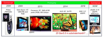
Solution processed light emitting organic materials were demonstrated in 1989 with a tiny 0.1 EQE (external quantum efficiency). Since then there has been tremendous progress on material synthesis/production as well as on display processing. However, thus far, commercialization has remained elusive.
In this article Dr Ghaffarzadeh will argue that the page may be about to turn. This could have important consequences for the large area display markets, especially if printing can enable a significant reduction in the production cost. This could reconfigure the landscape.
To learn about the details of the OLED industry please consult the IDTechEx Research report OLED Display Forecasts and Technologies 2019-2029: The Global Rise of Flexible and Foldable Displays. This report includes technology analysis and detailed forecasts by market segment and display type with additional assessment of printed OLEDs, Quantum Dot displays, E-Paper displays and other flexible displays.
The Limitations of Current Techniques
There are two main approaches today to OLED display production. Both utilize evaporated organics. In one, the emissive layers are evaporated through a fine metal mask (FMM) to achieve patterned side-by-side R, G, and B emitters. This approach works well for small up to medium sized displays. Indeed, today, it fully dominates the market for such products.
The technology however has proven difficult to scale up to large areas. The FMM is often made very thin to minimise shadowing effects during the evaporation. The downside of this thinness is that wide area masks become flimsy, easily sagging or warping under their own weight. This distorts the mask pattern. The FMM also, by definition, blocks and thus wastes 2/3 of the material. The blocked materials further add weight to the mask film, thus further complicating the situation.
Numerous approaches have been proposed to overcome these shortcomings, e.g., scanning the scanner over the substrate. None have, however, fully resolved the issues. Therefore, FMM has failed to transition to large area displays. To learn more about the market dynamics for OLED displays by technology, by device, and by flexibility type please see OLED Display Forecasts and Technologies 2019-2029: The Global Rise of Flexible and Foldable Displays.
The other approach is based upon white OLED (WOLED). Here, the organic layers are not patterned. Instead, they are blanket deposited. This way multiple OLED stacks are formed on top of one another to achieve white colour emission. In this approach, it is often common to have two blue layers to divide the drive voltage across two stacks whilst maintaining the brightness levels.
In general, WOLED involves depositing many layers. The RGB color effect comes from color filters. As such, the system has low efficiency (filters waste 2/3 of light). In turn, this demands higher brightness, leading to harsher drive conditions and shorter lifetimes. The primary advantage of this approach is that it can be scaled to large areas. This is why it is the technology of choice for OLED TVs. Reducing production cost however thus far has proven complicated although steady progress is being made. Consult the report OLED Display Forecasts and Technologies 2019-2029: The Global Rise of Flexible and Foldable Displays to learn more about WOLED technology and the OLED industry.
Both these approaches reply upon evaporated materials. An immediate question then is why is printing not being used. This way direct RGB patterning over large areas with high material utilization could be achieved. In the remainder of this article we will cover the progress and prospects of printing OLEDs.
Printed OLED Displays: Are the Materials Good Enough Yet?
Developing solution processible OLED materials has not been easy. At first, only polymeric materials could be solubilized. In the early generations, this would give very low EQEs and lifetimes. With time, polymer/small molecule and even solution-processible small molecule OLED materials were developed. The polymeric-only products also improved tremendously.
The upshot is that today after three decades of global research and development effort solution-processible OLEDs are becoming a viable proposition. Finally, the performance gap in Cd/A between leading printable OLEDs and commercial evaporated ones has been nearly bridged. This is true for green and red materials, and it is also the case for the blue with appropriate colour coordinates commonly used in displays.
Previously, any transition from evaporation to solution processing would impose a significant performance penalty. This no longer is necessarily the case. Therefore, the performance progress on the material side has eliminated, or at least strongly weakened, a major traditional reason against the adoption of printing.
The lifetime of solution OLEDs need to be further extended. An exact benchmarking is difficult because suppliers do not always speak the same language and mean different things by 'lifetime'. Each can use a different brightness level or lifetime definition (T90, T50, etc). Nonetheless, it is still the case that the lifetime of solution OLED materials lags behind evaporated ones. This gap will likely be closed with further development.
Page 1 of 2
Share on:


Testimonial
"We’re proud to call I-Connect007 a trusted partner. Their innovative approach and industry insight made our podcast collaboration a success by connecting us with the right audience and delivering real results."
Julia McCaffrey - NCAB GroupSuggested Items
KYZEN Honored with 2025 Step-by-Step Excellence Award for Its Innovative ANALYST² Process Control System
10/31/2025 | KYZEN'KYZEN, the global leader in innovative environmentally responsible cleaning chemistries, is proud to announce that its ANALYST² Process Control System has won a 2025 Step-by-Step Excellence Award (SbSEA).
LPKF Delivers Key Strategic Technology to Fraunhofer's Glass Panel Technology Group
10/29/2025 | LPKFLPKF Laser & Electronics SE is one of the initiators of the Glass Panel Technology Group (GPTG), a consortium encompassing the entire process chain for advanced semiconductor packaging with glass substrates.
On the Line With… Ultra HDI Podcast—Episode 7: “Solder Mask: Beyond the Traces,” Now Available
10/29/2025 | I-Connect007I-Connect007 is excited to announce the release of the seventh episode of its 12-part podcast series, On the Line With… American Standard Circuits: Ultra HDI. In this episode, “Solder Mask: Beyond the Traces,” host Nolan Johnson sits down with John Johnson, Director of Quality and Advanced Technology at American Standard Circuits, to explore the essential role that solder mask plays in the Ultra HDI (UHDI) manufacturing process.
Nvidia’s Blackwell Chips Made in Arizona Still Head to Taiwan for Final Assembly
10/27/2025 | I-Connect007 Editorial TeamNvidia has begun production of its next-generation Blackwell GPUs in the United States, but the company still depends heavily on Taiwan to complete the process, The Register reported.
American Standard Circuits Launches 50th 77-Second Webinar
10/27/2025 | American Standard CircuitsAnaya Vardya, President and CEO of American Standard Circuits/ASC Sunstone Circuits is pleased to announce that they have recently unveiled their 50th 77-second webinar.