


 Driving Innovation: Mechanical and Optical Processes During Rigid-flex Production
 It’s Only Common Sense: Your Biggest Competitor Is Complacency
 The Chemical Connection: Onshoring PCB Production—Daunting but Certainly Possible


Causes for Defects in 3D Printing
February 26, 2019 | Argonne National LaboratoryEstimated reading time: 6 minutes
Argonne/Carnegie Mellon team works to eliminate tiny pockets that cause big problems. Additive manufacturing’s promise to revolutionize industry is constrained by a widespread problem: tiny gas pockets in the final product, which can lead to cracks and other failures.
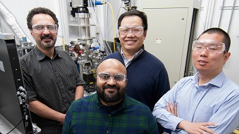
Image Caption: Argonne scientists who were co-authors on a recent paper about the 3D manufacturing process pose inside a hutch at Argonne’s Advanced Photon Source, in front of a specialty system that can simulate the Laser Powder Bed Fusion Process in a commercial 3D printer. Pictured, from top left, are Kamel Fezzaa, an APS beamline scientist; Tao Sun, an APS beamline scientist; Cang Zhao, an APS postdoc, and Niranjan Parab, an APS postdoc. (Image by Argonne National Laboratory.)
New research published today in Science, led by teams from Carnegie Mellon University and the U.S. Department of Energy’s (DOE) Argonne National Laboratory, has identified how and when these gas pockets form, as well as a methodology to predict their formation — information that could dramatically improve the 3D printing process.
“The research in this paper will translate into better quality and better control in working with the machines,” said Anthony Rollett, a Professor of Materials Science and Engineering at Carnegie Mellon University and an author on the paper. “For additive manufacturing to really take off for the majority of companies, we need to improve the consistency of the finished products. This research is a major step in that direction.”
The scientists used the extremely bright, high-energy X-rays at Argonne’s Advanced Photon Source (APS), a DOE Office of Science User Facility, to take super-fast video and images of a process called Laser Power Bed Fusion (LPBF), in which lasers are used to melt and fuse material powder together.
The lasers, which scan over each layer of powder to fuse metal where it is needed, literally create the finished product from the ground up. Defects can form when pockets of gas become trapped into these layers, causing imperfections that could lead to cracks or other breakdowns in the final product.
Until now, manufacturers and researchers did not know much about how the laser drills into the metal, producing cavities called “vapor depressions,” but they assumed that the type of metal powder or strength of laser were to blame. As a result, manufacturers have been using a trial and error approach with different types of metals and lasers to seek to reduce the defects.
In fact, the research shows that these vapor depressions exist under nearly all conditions in the process, no matter the laser or metal. Even more important, the research shows how to predict when a small depression will grow into a big and unstable one that can potentially create a defect.
“We’re drawing back the veil and revealing what’s really going on,” Rollett said. “Most people think you shine a laser light on the surface of a metal powder, the light is absorbed by the material, and it melts the metal into a melt pool. In actuality, you’re really drilling a hole into the metal.”
By using highly specialized equipment at Argonne’s APS, one of the most powerful synchrotron facilities in the world, researchers watched what happens as the laser moves across the metal powder bed to create each layer of the product.
Under perfect conditions, the melt pool shape is shallow and semicircular, called the “conduction mode.” But during the actual printing process, the high-power laser, often moving at a low speed, can change the melt pool shape to something like a keyhole in a warded lock: round and large on top, with a narrow spike at bottom. Such “keyhole mode” melting can potentially lead to defects in the final product.
This image, taken under the synchrotron at Argonne National Laboratory, shows a keyhole void about to be formed during the metal 3-D printing process. During laser powder bed fusion, a 3-D printer “drills” a hole into the metal. (Image courtesy of Carnegie Mellon University.)
“Based on this research, we now know that the keyhole phenomenon is more important, in many ways, than the powder being used in additive manufacturing,” said Ross Cunningham, a recent graduate from Carnegie Mellon University and one of the co-first authors of this paper. “Our research shows that you can predict the factors that lead to a keyhole — which means you can also isolate those factors for better results.”
The research shows that keyholes form when a certain laser power density is reached that is sufficient to boil the metal. This, in turn, reveals the critical importance of the laser focus in the additive manufacturing process, an element that has received scant attention so far, according to the research team.
“The keyhole phenomenon was able to be viewed for the first time with such details because of the specialized capability developed at Argonne,” said Tao Sun, an Argonne physicist and an author on the paper. “Of course, the intense high-energy X-ray beam at the APS is the key.”
The experiment platform that supports study of additive manufacturing includes a laser apparatus, specialized detectors, and dedicated beamline instruments.
In 2016, the Argonne team, together with their research partners, captured the first-ever X-ray video of laser additive manufacturing at micrometer and microsecond scales. That study increased interest in the techniques and the kinds of problems that could be researched at Argonne’s APS.
“We are really studying the most basic science problem, which is what happens to metal when you heat it up with a high-power laser,” said Cang Zhao, an Argonne postdoc and the other co-first author of the paper. “At the same time, because of our unique experimental capability, we are able to work with our collaborators on experiments that are really valuable to manufacturers.”
The research team believes this research could motivate makers of additive manufacturing machines to offer more flexibility when controlling the machines and that the improved use of the machines could lead to a significant improvement in the final product. In addition, if these insights are acted upon, the process for 3D printing could get faster.
“It’s important because 3D printing in general is rather slow,” Rollett said. “It takes hours to print a part that is a few inches high. That’s OK if you can afford to pay for the technique, but we need to do better.”
Co-lead authors are Ross Cunningham and Cang Zhao, from Carnegie Mellon University and Argonne National Laboratory, respectively; other authors from Carnegie Mellon University are Christopher Kantzos and Joseph Pauza; other authors from Argonne National Laboratory are Niranjan Parab and Kamel Fezzaa.
About the College of Engineering
The College of Engineering at Carnegie Mellon University is a top-ranked engineering college that is known for our intentional focus on cross-disciplinary collaboration in research. The College is well-known for working on problems of both scientific and practical importance. Our “maker” culture is ingrained in all that we do, leading to novel approaches and transformative results. Our acclaimed faculty have a focus on innovation management and engineering to yield transformative results that will drive the intellectual and economic vitality of our community, nation and world.
About Carnegie Mellon University
Carnegie Mellon is a private, internationally ranked university with programs in areas ranging from science, technology and business to public policy, the humanities and the arts. More than 13,000 students in the university’s seven schools and colleges benefit from a small faculty-to-student ratio and an education characterized by its focus on creating and implementing solutions for real world problems, interdisciplinary collaboration and innovation.
Share on:


Testimonial
"Your magazines are a great platform for people to exchange knowledge. Thank you for the work that you do."
Simon Khesin - Schmoll MaschinenSuggested Items
Unlocking the Promise of AI in Electronics Manufacturing
10/29/2025 | Shobhit Agrawal, Keysight TechnologiesThe electronics manufacturing industry is rapidly evolving as more complicated products are introduced in the production lines, which require technological advancements even in the production processes. The requirements for production that is efficient, product quality that is greater, and product life cycles that are shorter are more crucial than ever before. In the electronic device life cycle, from design to maintenance, test phases have a significant impact on the economy of the company. Test processes are closely linked to the production volume and impacted by the complexity of the product. For businesses to maintain their competitive edge, they need to adopt innovative solutions and redefine processes.
Driving Innovation: Mechanical and Optical Processes During Rigid-flex Production
10/28/2025 | Kurt Palmer -- Column: Driving InnovationRigid-flex printed circuit boards are a highly effective solution for placing complex circuitry in tight, three-dimensional spaces. They are now indispensable across a range of industries, from medical devices and aerospace to advanced consumer electronics, helping designers make the most efficient use of available space. However, their unique construction—combining rigid and flexible materials—presents a fundamental challenge for PCB manufacturers.
SMTAI 2025 Review: Reflecting on a Pragmatic and Forward-looking Industry
10/27/2025 | Marcy LaRont, I-Connect007Leaving the show floor on the final afternoon of SMTA International last week in Rosemont, Illinois, it was clear that the show remains a grounded, technically driven event that delivers a solid program, good networking, and an easy space to commune with industry colleagues and meet with customers.
The Marketing Minute: Marketing With Layers
10/15/2025 | Brittany Martin -- Column: The Marketing MinuteMarketing to a technical audience is like crafting a multilayer board: Each layer serves a purpose, from the surface story to the buried detail that keeps everything connected. At I-Connect007, we’ve learned that the best marketing campaigns aren’t built linearly; they’re layered. A campaign might start with a highly technical resource, such as an in-depth article, a white paper, or a podcast featuring an engineer delving into the details of a process. That’s the foundation, the substance that earns credibility.
Taking Control of PCB Verification One Step at a Time
10/09/2025 | Kirk Fabbri, Siemens EDAToday’s designs are as complex as ever, and engineers face tough decisions every day. Simulation and verification teams are confronted with a three-fold challenge: understanding the underlying theory, mastering the tools, and applying best practices.Engineers need to navigate a vast and ever-changing cast of design and simulation tools, often with overlapping functionality.