


 Driving Innovation: Mechanical and Optical Processes During Rigid-flex Production
 It’s Only Common Sense: Your Biggest Competitor Is Complacency
 The Chemical Connection: Onshoring PCB Production—Daunting but Certainly Possible


Smoothing Out the Wrinkles in Graphene
March 7, 2019 | MITEstimated reading time: 4 minutes
To protect graphene from performance-impairing wrinkles and contaminants that mar its surface during device fabrication, MIT researchers have turned to an everyday material: wax.
Graphene is an atom-thin material that holds promise for making next-generation electronics. Researchers are exploring possibilities for using the exotic material in circuits for flexible electronics and quantum computers, and in a variety of other devices.
But removing the fragile material from the substrate it’s grown on and transferring it to a new substrate is particularly challenging. Traditional methods encase the graphene in a polymer that protects against breakage but also introduces defects and particles onto graphene’s surface. These interrupt electrical flow and stifle performance.
In a paper published in Nature Communications, the researchers describe a fabrication technique that applies a wax coating to a graphene sheet and heats it up. Heat causes the wax to expand, which smooths out the graphene to reduce wrinkles. Moreover, the coating can be washed away without leaving behind much residue.
In experiments, the researchers’ wax-coated graphene performed four times better than graphene made with a traditional polymer-protecting layer. Performance, in this case, is measured in “electron mobility” — meaning how fast electrons move across a material’s surface — which is hindered by surface defects.
“Like waxing a floor, you can do the same type of coating on top of large-area graphene and use it as layer to pick up the graphene from a metal growth substrate and transfer it to any desired substrate,” says first author Wei Sun Leong, a postdoc in the Department of Electrical Engineering and Computer Science (EECS). “This technology is very useful, because it solves two problems simultaneously: the wrinkles and polymer residues.”
Co-first author Haozhe Wang, a PhD student in EECS, says using wax may sound like a natural solution, but it involved some thinking outside the box — or, more specifically, outside the laboratory: “As students, we restrict ourselves to sophisticated materials available in lab. Instead, in this work, we chose a material that commonly used in our daily life.”
Joining Leong and Wang on the paper are: Jing Kong and Tomas Palacios, both EECS professors; Markus Buehler, professor and head of the Department of Civil and Environmental Engineering (CEE); and six other graduate students, postdocs, and researchers from EECS, CEE, and the Department of Mechanical Engineering.
The “Perfect” Protector
To grow graphene over large areas, the 2-D material is typically grown on a commercial copper substrate. Then, it’s protected by a “sacrificial” polymer layer, typically polymethyl methacrylate (PMMA). The PMMA-coated graphene is placed in a vat of acidic solution until the copper is completely gone. The remaining PMMA-graphene is rinsed with water, then dried, and the PMMA layer is ultimately removed.
Wrinkles occur when water gets trapped between the graphene and the destination substrate, which PMMA doesn’t prevent. Moreover, PMMA comprises complex chains of oxygen, carbon, and hydrogen atoms that form strong bonds with graphene atoms. This leaves behind particles on the surface when it’s removed.
Researchers have tried modifying PMMA and other polymers to help reduce wrinkles and residue, but with minimal success. The MIT researchers instead searched for completely new materials — even once trying out commercial shrink wrap. “It was not that successful, but we did try,” Wang says, laughing.
After combing through materials science literature, the researchers landed on paraffin, the common whitish, translucent wax used for candles, polishes, and waterproof coatings, among other applications.
In simulations before testing, Buehler’s group, which studies the properties of materials, found no known reactions between paraffin and graphene. That’s due to paraffin’s very simple chemical structure. “Wax was so perfect for this sacrificial layer. It’s just simple carbon and hydrogen chains with low reactivity, compared to PMMA’s complex chemical structure that bonds to graphene,” Leong says.
Cleaner Transfer
In their technique, the researchers first melted small pieces of the paraffin in an oven. Then, using a spin coater, a microfabrication machine that uses centrifugal force to uniformly spread material across a substrate, they dropped the paraffin solution onto a sheet of graphene grown on copper foil. This spread the paraffin into a protective layer, about 20 microns thick, across the graphene.
The researchers transferred the paraffin-coated graphene into a solution that removes the copper foil. The coated graphene was then relocated to a traditional water vat, which was heated to about 40 degrees Celsius. They used a silicon destination substrate to scoop up the graphene from underneath and baked in an oven set to the same temperature.
Because paraffin has a high thermal expansion coefficient, it expands quite a lot when heated. Under this heat increase, the paraffin expands and stretches the attached graphene underneath, effectively reducing wrinkles. Finally, the researchers used a different solution to wash away the paraffin, leaving a monolayer of graphene on the destination substrate.
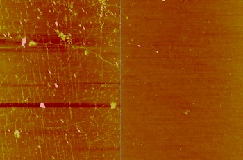
In their paper, the researchers show microscopic images of a small area of the paraffin-coated and PMMA-coated graphene. Paraffin-coated graphene is almost fully clear of debris, whereas the PMMA-coated graphene looks heavily damaged, like a scratched window.
Because wax coating is already common in many manufacturing applications — such as applying a waterproof coating to a material — the researchers think their method could be readily adapted to real-world fabrication processes. Notably, the increase in temperature to melt the wax shouldn’t affect fabrication costs or efficiency, and the heating source could in the future be replaced with a light, the researchers say.
Next, the researchers aim to further minimize the wrinkles and contaminants left on the graphene and scaling up the system to larger sheets of graphene. They’re also working on applying the transfer technique to the fabrication processes of other 2-D materials.
“We will continue to grow the perfect large-area 2-D materials, so they come naturally without wrinkles,” Leong says.
Share on:


Testimonial
"Our marketing partnership with I-Connect007 is already delivering. Just a day after our press release went live, we received a direct inquiry about our updated products!"
Rachael Temple - AlltematedSuggested Items
WestDev Announces Advanced Thermal Analysis Integration for Pulsonix PCB Design Suite
10/29/2025 | WestDev Ltd.Pulsonix, the industry-leading PCB design software from WestDev Ltd., announced a major enhancement to its design ecosystem: a direct interface between Pulsonix and ADAM Research's TRM (Thermal Risk Management) analysis software.
Designers Notebook: Power and Ground Distribution Basics
10/29/2025 | Vern Solberg -- Column: Designer's NotebookThe principal objectives to be established during the planning stage are to define the interrelationship between all component elements and confirm that there is sufficient surface area for placement, the space needed to ensure efficient circuit interconnect, and to accommodate adequate power and ground distribution.
Episode 6 of Ultra HDI Podcast Series Explores Copper-filled Microvias in Advanced PCB Design and Fabrication
10/15/2025 | I-Connect007I-Connect007 has released Episode 6 of its acclaimed On the Line with... American Standard Circuits: Ultra High Density Interconnect (UHDI) podcast series. In this episode, “Copper Filling of Vias,” host Nolan Johnson once again welcomes John Johnson, Director of Quality and Advanced Technology at American Standard Circuits, for a deep dive into the pros and cons of copper plating microvias—from both the fabricator’s and designer’s perspectives.
Nolan’s Notes: Tariffs, Technologies, and Optimization
10/01/2025 | Nolan Johnson -- Column: Nolan's NotesLast month, SMT007 Magazine spotlighted India, and boy, did we pick a good time to do so. Tariff and trade news involving India was breaking like a storm surge. The U.S. tariffs shifted India from one of the most favorable trade agreements to the least favorable. Electronics continue to be exempt for the time being, but lest you think that we’re free and clear because we manufacture electronics, steel and aluminum are specifically called out at the 50% tariff levels.
MacDermid Alpha & Graphic PLC Lead UK’s First Horizontal Electroless Copper Installation
09/30/2025 | MacDermid Alpha & Graphic PLCMacDermid Alpha Electronics Solutions, a leading supplier of integrated materials and chemistries to the electronics industry, is proud to support Graphic PLC, a Somacis company, with the installation of the first horizontal electroless copper metallization process in the UK.