


 Dan’s Biz Bookshelf: ‘Abundance: How We Build a Better Future’
 Trouble in Your Tank: In Complex Systems, Design Rules Aren’t Optional
 It’s Only Common Sense: The Phone Is Still Your Competitive Advantage


Mass Manufacturing of Metasurfaces
March 18, 2019 | A*STAREstimated reading time: 2 minutes
The mass production of flat optical devices with sub-wavelength structures could soon be a reality, thanks to a metasurface fabrication technique developed by researchers at A*STAR.
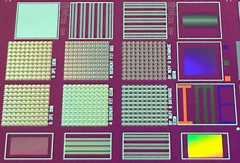
Image Caption: The metasurface's nano-pillar arrays displaying the letters I, M and E in red, green and blue, respectively. (The Optical Society)
Metasurfaces are synthetic, two-dimensional materials covered in tiny individual shapes with sizes and spacings smaller than the wavelengths of visible light. These ‘sub-wavelength’ structures enable scientists to precisely control the propagating shape, or wavefront, of light beams. As such, metasurfaces show promise for many applications from high-resolution imaging and color printing to controlling light polarization. Mass production of metasurfaces, however, has proven challenging, limited by the complexity of realizing such precise patterns.
Now, Ting Hu and his colleagues at A*STAR’s Institute of Microelectronics (IME) have developed a method of building silicon-based metasurfaces by introducing existing techniques from semiconductor fabrication. Their new metasurface design can produce high-resolution red-green-blue (RGB) color displays.
Until now, metasurfaces have mainly been fabricated via electron beam lithography (EBL), which is not applicable to mass production, as Hu explains:
“With EBL, the focused electron beam moves slowly, step by step, across the metasurface substrate. Metasurfaces with millions — possibly billions — of elements require a very long time to be patterned via EBL. We desired a faster and more efficient way of patternation.”
Hu and the team based their technique on ‘immersion lithography’, which has long been used to etch patterns on to electronic components. With multiple exposures, complex patterns can be built up. The researchers used ultraviolet-based (UV) lithography for initial patternation on to silicon substrates, followed by plasma etching to form the designs in small pixel blocks that were assembled into a 12-inch display surface (see image).
“Our UV lithography tool is a scanner, which can pattern a whole 12 inch wafer with designed devices within half an hour,” says Hu. “We designed the physical dimensions of the nano-pillar arrays of the metasurface to accurately display colors, with fantastic results, for example displaying the letters I, M and E in red, green and blue respectively.”
Hu and the team hope to optimize their design and improve the etching process to minimize losses induced by light scattering and defects in the nano-structure arrays. They are also making efforts to realize flat, lightweight ‘meta-lenses’ and dot projectors with potential uses in facial recognition technologies.
Share on:


Subscribe
Stay ahead of the technologies shaping the future of electronics with our latest newsletter, Advanced Electronics Packaging Digest. Get expert insights on advanced packaging, materials, and system-level innovation, delivered straight to your inbox.
Subscribe now to stay informed, competitive, and connected.
Suggested Items
Gregoire Outters Promoted to President of Teledyne Marine Group
04/06/2026 | TeledyneTeledyne Technologies Incorporated announced the promotion of Gregoire Outters to President of its Teledyne Marine Group.
Teledyne Strengthens Commitment to the Space Sector
04/01/2026 | BUSINESS WIRETeledyne Technologies Incorporated is excited to announce the integration of the company’s extensive portfolio of space-focused technologies and businesses, reinforcing its long-term commitment to the global space sector.
Teledyne to Supply Detectors for Lazuli Space Observatory
03/30/2026 | BUSINESS WIRETeledyne Space Imaging, part of Teledyne Technologies Incorporated has been awarded a contract by Schmidt Sciences to deliver advanced near-infrared (NIR) H4RG-10 flight focal plane arrays (FPAs) and custom electronics for integration into the Integral Field Spectrograph on the groundbreaking Lazuli Space Observatory.
New Superconducting Chip Could Enable Breakthrough Nondestructive Terahertz Imaging
03/23/2026 | University of GlasgowA tiny crystal chip which uses terahertz radiation to see clearly through a wide range of materials could find applications in healthcare, biological research, and security screening.
The Test Connection Adds Creative Electron Prime TruVision™ X-ray and CT System for Deeper Failure Analysis
03/05/2026 | TTCIThe Test Connection Inc. (TTCI), a trusted provider of electronic test and manufacturing solutions for more than 45 years, has added the Prime TruVision™ X-ray and computed tomography (CT) inspection system from Creative Electron to its engineering and analysis services.