


 Dan’s Biz Bookshelf: ‘Abundance: How We Build a Better Future’
 Trouble in Your Tank: In Complex Systems, Design Rules Aren’t Optional
 It’s Only Common Sense: The Phone Is Still Your Competitive Advantage


Rendering a 2D Perovskite Template into a 3D Film
March 22, 2019 | University of GroningenEstimated reading time: 2 minutes
Formamidinium lead iodide is a very good material for photovoltaic cells, but getting the correct and stable crystal structure is a challenge. The techniques developed so far have produced rather poor results. However, University of Groningen scientists, led by Professor of Photophysics and Optoelectronics Maria Antonietta Loi, have now cracked it—using a blade and a dipping solution.
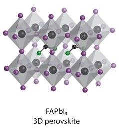
Formamidinium lead iodide (FAPbI3) is a perovskite, a crystal with a distinctive structure. Perovskites are named after a mineral that has the chemical formula ABX3. In an idealized cubic unit cell, the X position is occupied by anions that form an octahedron with a central cation in the B position while the corners of the cube are occupied by the A position cations (see picture).
Image Caption: The 2D films based on 2-phenylethylammonium lead iodide produce 3D formamidinium lead iodide films via cation exchange.
Industrial Production
'This formamidinium lead iodide material has very good characteristics, but the A position formamidinium ion causes instability in the structure,' explains Loi. 3D films made from this material most often turn out to be a mixture of a photoactive and a photoinactive phase, the latter being detrimental to the final application. Loi therefore set her PhD student Sampson Adjokatse to work to find a solution.
After trying different strategies, he found one that worked. 'And most importantly, one that is scalable and could be used for industrial production,' says Loi. After all, solar cells must be produced in large panels and it is very important to find a good and cheap technique to do so. Adjokatse started with a different perovskite, in which the formamidinium was replaced by a larger 2 phenylethylammonium molecule, and in doing so formed a 2D perovskite. This material was deposited as a thin film using the 'doctor-blade' technique, related to techniques widely used in industrial processes such as printing.
Blade
'Basically, you spread the material onto a substrate using a blade,' explains Adjokatse. The blade can be set to produce a film with a thickness of around 500 nanometres, creating the 2D perovskite layer. 'The important point is that these films are very smooth with large crystalline domains of up to 15 micrometres,' says Adjokatse. The smooth 2D films based on 2-phenylethylammonium lead iodide were used as a template to produce 3D formamidinium lead iodide films.
This was achieved by dipping the 2D film in a solution containing formamidinium iodide. This resulted in the growth of a 3D film through 'cation exchange', where formamidinium took the place of 2 phenylethylammonium. 'These films show much higher photoluminescence compared to reference 3D formamidinium lead iodide films and show increased stability when exposed to light or moisture,' says Loi. 'This means that we now have a method for the production of high-quality films for perovskite solar cells using an industrially scalable technique.'
Share on:


Subscribe
Stay ahead of the technologies shaping the future of electronics with our latest newsletter, Advanced Electronics Packaging Digest. Get expert insights on advanced packaging, materials, and system-level innovation, delivered straight to your inbox.
Subscribe now to stay informed, competitive, and connected.
Suggested Items
MacDermid Alpha to Debut Zero-PFAS Die Attach Paste ATROX CD 560-1 at SEMICON Southeast Asia 2026
04/27/2026 | MacDermid Alpha Electronics SolutionsMacDermid Alpha Electronics Solutions will debut ATROX® CD 560-1, a zero-PFAS conductive die attach paste, at SEMICON Southeast Asia 2026, May 5–7, in Kuala Lumpur, Booth 2423.
Infineon Further Extends Global Leadership in the Automotive Semiconductor Market
04/13/2026 | InfineonInfineon Technologies AG has once again proven to be the world’s leading automotive semiconductor supplier.
OKI Launches EMS for AI Server Equipment Featuring Proprietary High Heat Dissipation Technology
04/07/2026 | BUSINESS WIREOKI will launch Comprehensive Electronics Manufacturing Services (EMS) for AI server equipment on March 25, 2026.
The Right Approach: Reflections on 50 Years in the Business, Part 3
03/31/2026 | Steve Williams -- Column: The Right ApproachWaking up that first day in 2013 after being informed my position of 15 years had been eliminated, I realized that everything I had done in my career had positioned me for a new chapter. This included the hands-on leadership experience in PCB manufacturing, learning from over 1,000 global companies, and my industry exposure while working at Plexus. My passion for writing, educating, speaking, and passing along my experience to others made it clear that this was the time to pursue my dream job: owning a consulting company.
OKI Launches EMS for AI Server Equipment Featuring Proprietary High Heat Dissipation Technology
03/25/2026 | BUSINESS WIREOKI will launch Comprehensive Electronics Manufacturing Services (EMS) for AI server equipment on March 25, 2026.