


 Dan’s Biz Bookshelf: ‘Abundance: How We Build a Better Future’
 Trouble in Your Tank: In Complex Systems, Design Rules Aren’t Optional
 It’s Only Common Sense: The Phone Is Still Your Competitive Advantage


Controlling Nuclear Noise in Semiconductor Qubits
March 27, 2019 | IBMEstimated reading time: 2 minutes
When it comes to quantum computation, superconducting qubits are currently leading the field. But there are other ways to represent a qubit. The spin of an electron is arguably a much simpler object than a superconducting circuit: In a straightforward way, spin up and spin down represent the two qubit states, 0 and 1. However, also for spin qubits, the stored quantum information does not persist forever. The electrons interact with their environment and thereby lose their spin polarization over time.
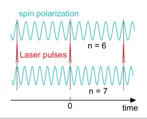
Image Caption: Principle of spin locking: A periodic laser pulse train locks the spin precession frequency to an integer multiple n of the laser repetition rate. In the example, the spins precess either exactly n = 6 or n = 7 times between two subsequent laser pulses.
Electron spins are typically captured on semiconductor “islands” (so-called quantum dots) that consist of more than 100,000 atoms. Depending on the material used, the atomic nuclei may have a spin themselves. Each nuclear spin slightly modifies the energy of the electron spin. This by itself would not be a problem. It however becomes an issue because the nuclear spins randomly change their direction over time and with this the energy of the qubit starts to fluctuate.
Different techniques have been developed to get such fluctuations under control and keep the nuclear spin polarization constant. A very intriguing possibility consists in illuminating the semiconductor island with periodic laser pulses. It has been found that such illumination brings the qubit energy to a well-defined value that is directly related to the laser repetition rate. Such a locking of the qubit energy has been observed in quantum dots that contain a single electron, but the exact reason why the energy locks to the laser repetition rate has remained unclear.
Image Caption: The color in this image encodes the spin polarization along a fixed direction in space, measured on semiconductor quantum dots by the IBM team. The spins oscillate at a frequency that can be varied by a magnetic field. The sample is illuminated with periodic laser pulses. Time zero marks the moment when a laser pulse arrives at the dot. The spin oscillation is locked to the laser repetition rate irrespective of the applied magnetic field.
Together with collaborators at ETH Zurich, our team at IBM Research – Zurich has investigated this effect and has found that it is much more universal than previously thought: We could observe nuclear focusing also in islands that contain many electron spins and that are fabricated using standard techniques of the semiconductor industry. We found that the optical Stark effect is responsible for the nuclear focusing: Each laser pulse creates a short-lived and tiny magnetic field that slowly steers the nuclear spins into a well-defined polarization. This became clear when we changed the energy of the laser pulses. With a lower energy, the direction of the tiny magnetic field reverses and with it the electron spins become anti-locked with the laser repetition rate, which is well explained by the model.
With this technique, the lifetime of the spin qubit can be substantially prolonged beyond the limit given by the fluctuating nuclear spins. As we have shown, nuclear focusing also works in quantum dots carved out of a semiconductor material using lithography and etching techniques. With this, dots of well-controlled shape, size and position can be fabricated, which is essential to apply this technique to spin qubits in a scalable way.
Share on:


Subscribe
Stay ahead of the technologies shaping the future of electronics with our latest newsletter, Advanced Electronics Packaging Digest. Get expert insights on advanced packaging, materials, and system-level innovation, delivered straight to your inbox.
Subscribe now to stay informed, competitive, and connected.
Suggested Items
Institute of Circuit Technology Spring Seminar 2026: A Bright Future in Europe
04/23/2026 | Pete Starkey, I-Connect007Through the leafy lanes and spring flowers of Warwickshire and back to Meridan, the traditional centre of England, and now officially part of the Metropolitan Borough of Solihull in the county of the West Midlands, I attended the Annual General Meeting and Spring Seminar of the Institute of Circuit Technology (ICT) on April 14. Out of the AGM came notable changes in leadership at the top of the Institute: the retirement of Mat Beadel as chair and Emma Hudson as technical director. Effective May 1, Steve Driver is the new chair, and Alun Morgan is the new technical director.
Henger Targets AI PCB Challenges With Advanced Plasma Technology
04/02/2026 | I-Connect007 Editorial TeamHenger is pushing the boundaries of PCB manufacturing with its dynamic, next-generation plasma technology, purpose-built for the demands of AI-driven electronics. As designs move toward higher density, faster speeds, and advanced materials like M9 laminates, Henger’s innovative plasma systems deliver precise, uniform, and energy-efficient processing. In this interview, company leaders, Zhiquang Li and Ping Tang discuss how their cutting-edge solutions are redefining cleaning, surface activation, and process control—positioning plasma technology as a critical enabler of reliability and performance in the rapidly evolving AI hardware landscape.
New, Greener Solutions for Etch: Novel Copper Extraction
03/30/2026 | Richard Nichols, GreenSource Engineering“Novel” is a typical marketing phrase that implies new and unique, but often “novel” actually means an established technology being applied to a new field or application. This, in turn, is often driven by newly relevant external motivation. GreenSource has been working on just such a solution: novel copper extraction, offering a better and greener alternative to traditional LLE control systems for cupric chloride etch.
Connect the Dots: Designing for the Future of Manufacturing Reality—Strip-Etch-Strip
02/19/2026 | Matt Stevenson -- Column: Connect the DotsThe demand for ultra-high density interconnect (UHDI) PCBs is growing as electronic devices become increasingly advanced. That means we will be creating more designs that need to align with the reality of manufacturing UHDI boards. My last column on this subject focused on plating, and we are ready to discuss the strip-etch-strip (SES) process. With UHDI boards, footprints are smaller and tolerances are tighter. Your big design challenge associated with the SES process involves trace width and spacing control. The etching process can undercut traces and alter their final size.
PCBAIR Upgrades Heavy-Copper PCBs to Solve AI Thermal Bottlenecks
01/20/2026 | PRNewswireAs computational demands for AI models surge, the hardware powering them faces a critical physical limitation: thermal management.