


 Dan’s Biz Bookshelf: ‘Abundance: How We Build a Better Future’
 Trouble in Your Tank: In Complex Systems, Design Rules Aren’t Optional
 It’s Only Common Sense: The Phone Is Still Your Competitive Advantage


Researchers Develop High-Resolution, High-Sensitivity Proximity Capacitance Imaging Sensor
April 8, 2019 | Tohoku UniversityEstimated reading time: 3 minutes
A fingerprint can serve as identification to access locked doors and more, but current scanners can be duped with fake or even similar fingerprints. That may change soon, thanks to a collaborative research team based in Japan.
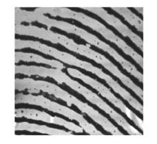
Proximity capacitance image of a fingerprint. The captured image clearly shows not only the fingerprint, but also sweat pores of the skin. Shigetoshi Sugawa, Tohoku University
The group has developed a new proximity capacitance imaging sensor that has such high sensitivity and resolution, a finger print scan shows more than the swirls of a fingertip—it detects the sweat pores between the ridges.
The prototype sensor was first presented in December at the 2018 IEEE International Electron Devices Meeting in San Francisco, California. A paper describing the details of the sensor was published in the Technical Digests of 2018 International Electron Devices Meeting. Last week, the authors presented new materials and results from the study at a conference organized by the Institute of Image Information and Television Engineers (ITE) in Japan.
"The most significant point of the developed sensor is its high capacitance sensitivity," said paper author Shigetoshi Sugawa, a professor in the Graduate School of Engineering at Tohoku University.
Many touch screen phones and computer track pads use a less sensitive capacitance sensor, where the differences in electrical properties between a sensor and a conductive tool (such as a finger) allow the device to react to scrolling or double clicking. The capacitance increases when the object is closer—the double-click versus lighter scrolling.
The high sensitivity of this capacitance sensor is derived from newly introduced noise reduction technology, according to Sugawa.
Prototype in precision
The sensor chip contains pixels to detect the capacitance between the sample and detection electrodes. Each pixel has one detection electrode attached to it that's capacitively coupled with a ground wire. These electrical signals are converted into images of the samples. Previously, the signals would pick up background noise such as thermal noise and noise due to variability of electrical components of pixels, which made for lower-quality images.
To fix this, the researchers applied reset switches to the detection electrodes and employed a voltage pulse to produce a circuit that can follow the source of noise. The reset switches allow the systems to detect noise arising at the detection electrodes. The voltage pulse alternates the two voltage levels after the reset switches are turned off, effectively cancelling out and removing noise from the system.
It's the equivalent of removing the white and black snow from a television without signal input into a smooth, grey screen. It's much easier to sense any deviation on a solid background.
"This development is important to the general public because it can improve the efficiency of analysis and control in the fields of electronic industry, authentication, life sciences, agriculture, and more," Sugawa said.
Next, Sugawa and the researchers plan to optimize the sensor for specific applications, such as the non-contact inspection equipment of printed circuit boards and flat panels as well as a portable camera system with the developed sensor chip.
The research team consists of Sugawa, as well as Rihito Kuroda, an associate professor, Masahiro Yamamoto, Manabu Suzuki, graduate students both with the Tohoku University's Graduate School of Engineering; Tetsuya Goto, an associate professor with Tohoku University's New Industry Creation Hatchery Center; Hiroshi Hamori, president, Shinichi Murakami and Toshiro Yasuda, at OHT, Inc.
The prototype sensor was first presented in December at the 2018 IEEE International Electron Devices Meeting in San Francisco, California. A paper describing the details of the sensor was published in the Technical Digests of 2018 International Electron Devices Meeting. On March 22, the authors presented new materials and results from the study at a conference organized by the Institute of Image Information and Television Engineers (ITE) in Japan.
Share on:


Subscribe
Stay ahead of the technologies shaping the future of electronics with our latest newsletter, Advanced Electronics Packaging Digest. Get expert insights on advanced packaging, materials, and system-level innovation, delivered straight to your inbox.
Subscribe now to stay informed, competitive, and connected.
Suggested Items
Gregoire Outters Promoted to President of Teledyne Marine Group
04/06/2026 | TeledyneTeledyne Technologies Incorporated announced the promotion of Gregoire Outters to President of its Teledyne Marine Group.
Teledyne Strengthens Commitment to the Space Sector
04/01/2026 | BUSINESS WIRETeledyne Technologies Incorporated is excited to announce the integration of the company’s extensive portfolio of space-focused technologies and businesses, reinforcing its long-term commitment to the global space sector.
Teledyne to Supply Detectors for Lazuli Space Observatory
03/30/2026 | BUSINESS WIRETeledyne Space Imaging, part of Teledyne Technologies Incorporated has been awarded a contract by Schmidt Sciences to deliver advanced near-infrared (NIR) H4RG-10 flight focal plane arrays (FPAs) and custom electronics for integration into the Integral Field Spectrograph on the groundbreaking Lazuli Space Observatory.
New Superconducting Chip Could Enable Breakthrough Nondestructive Terahertz Imaging
03/23/2026 | University of GlasgowA tiny crystal chip which uses terahertz radiation to see clearly through a wide range of materials could find applications in healthcare, biological research, and security screening.
The Test Connection Adds Creative Electron Prime TruVision™ X-ray and CT System for Deeper Failure Analysis
03/05/2026 | TTCIThe Test Connection Inc. (TTCI), a trusted provider of electronic test and manufacturing solutions for more than 45 years, has added the Prime TruVision™ X-ray and computed tomography (CT) inspection system from Creative Electron to its engineering and analysis services.