


 Dan’s Biz Bookshelf: ‘Abundance: How We Build a Better Future’
 Trouble in Your Tank: In Complex Systems, Design Rules Aren’t Optional
 It’s Only Common Sense: The Phone Is Still Your Competitive Advantage


Researchers 3D Print Metamaterials With Novel Optical Properties
April 8, 2019 | Tufts UniversityEstimated reading time: 3 minutes
A team of engineers at Tufts University has developed a series of 3D printed metamaterials with unique microwave or optical properties that go beyond what is possible using conventional optical or electronic materials. The fabrication methods developed by the researchers demonstrate the potential, both present and future, of 3D printing to expand the range of geometric designs and material composites that lead to devices with novel optical properties.
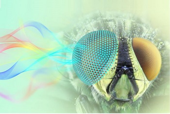
The geometry of a moth's eye provides inspiration for a 3D printed antenna that absorbs specific microwave frequencies from any direction. Credit: Hojat Nejad
In one case, the researchers drew inspiration from the compound eye of a moth to create a hemispherical device that can absorb electromagnetic signals from any direction at selected wavelengths. The research was published today in the journal Microsystems & Nanoengineering, published by Springer Nature.
Metamaterials extend the capabilities of conventional materials in devices by making use of geometric features arranged in repeating patterns at scales smaller than the wavelengths of energy being detected or influenced. New developments in 3D printing technology are making it possible to create many more shapes and patterns of metamaterials, and at ever smaller scales. In the study, researchers at the Nano Lab at Tufts describe a hybrid fabrication approach using 3D printing, metal coating and etching to create metamaterials with complex geometries and novel functionalities for wavelengths in the microwave range.
For example, they created an array of tiny mushroom shaped structures, each holding a small patterned metal resonator at the top of a stalk. This particular arrangement permits microwaves of specific frequencies to be absorbed, depending on the chosen geometry of the “mushrooms” and their spacing. Use of such metamaterials could be valuable in applications such as sensors in medical diagnosis and as antennas in telecommunications or detectors in imaging applications.
Other devices developed by the authors include parabolic reflectors that selectively absorb and transmit certain frequencies. Such concepts could simplify optical devices by combining the functions of reflection and filtering into one unit. “The ability to consolidate functions using metamaterials could be incredibly useful,” said Sameer Sonkusale, professor of electrical and computer engineering at Tufts University’s School of Engineering who heads the Nano Lab at Tufts and is corresponding author of the study. “It’s possible that we could use these materials to reduce the size of spectrometers and other optical measuring devices so they can be designed for portable field study.”
The products of combining optical/electronic patterning with 3D fabrication of the underlying substrate are referred to by the authors as metamaterials embedded with geometric optics, or MEGOs. Other shapes, sizes, and orientations of patterned 3D printing can be conceived to create MEGOs that absorb, enhance, reflect or bend waves in ways that would be difficult to achieve with conventional fabrication methods.
There are a number of technologies now available for 3D printing, and the current study utilizes stereolithography, which focuses light to polymerize photo-curable resins into the desired shapes. Other 3D printing technologies, such as two photon polymerization, can provide printing resolution down to 200 nanometers, which enables the fabrication of even finer metamaterials that can detect and manipulate electromagnetic signals of even smaller wavelengths, potentially including visible light.
“The full potential of 3D printing for MEGOs has not yet been realized,” said Aydin Sadeqi, graduate student in Sankusale’s lab at Tufts University School of Engineering and lead author of the study. “There is much more we can do with the current technology, and a vast potential as 3D printing inevitably evolves.”
Other authors contributing to the research include Hojatollah Rezaei Nejad, post-doctoral fellow, and Rachel Owyeung, graduate student at Tufts University School of Engineering.
Share on:


Subscribe
Stay ahead of the technologies shaping the future of electronics with our latest newsletter, Advanced Electronics Packaging Digest. Get expert insights on advanced packaging, materials, and system-level innovation, delivered straight to your inbox.
Subscribe now to stay informed, competitive, and connected.
Suggested Items
Gregoire Outters Promoted to President of Teledyne Marine Group
04/06/2026 | TeledyneTeledyne Technologies Incorporated announced the promotion of Gregoire Outters to President of its Teledyne Marine Group.
Teledyne Strengthens Commitment to the Space Sector
04/01/2026 | BUSINESS WIRETeledyne Technologies Incorporated is excited to announce the integration of the company’s extensive portfolio of space-focused technologies and businesses, reinforcing its long-term commitment to the global space sector.
Teledyne to Supply Detectors for Lazuli Space Observatory
03/30/2026 | BUSINESS WIRETeledyne Space Imaging, part of Teledyne Technologies Incorporated has been awarded a contract by Schmidt Sciences to deliver advanced near-infrared (NIR) H4RG-10 flight focal plane arrays (FPAs) and custom electronics for integration into the Integral Field Spectrograph on the groundbreaking Lazuli Space Observatory.
New Superconducting Chip Could Enable Breakthrough Nondestructive Terahertz Imaging
03/23/2026 | University of GlasgowA tiny crystal chip which uses terahertz radiation to see clearly through a wide range of materials could find applications in healthcare, biological research, and security screening.
The Test Connection Adds Creative Electron Prime TruVision™ X-ray and CT System for Deeper Failure Analysis
03/05/2026 | TTCIThe Test Connection Inc. (TTCI), a trusted provider of electronic test and manufacturing solutions for more than 45 years, has added the Prime TruVision™ X-ray and computed tomography (CT) inspection system from Creative Electron to its engineering and analysis services.