


 Powering the Future: Why True Ceramic Circuits Are Not Just ‘Better PCBs’
 Global Sourcing Spotlight: The Global Quality Gap—Why Consistency Wins the Contract
 Knocking Down the Bone Pile: Precision Milling of Underfilled SMT Components


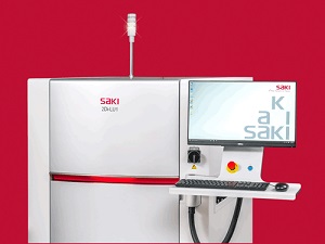
Saki Corporation announces the release of its new 2Di-LU1 inline bottom-side automated optical inspection (AOI) system at NEPCON China, Shanghai, China, and SMTconnect, Nuremberg, Germany. Saki's 2D line-scan technology is ultra-fast, capturing the image of an entire 460x500mm printed circuit board assembly (PCBA) and carriers of 610x610mm in one pass, in real time, storing the image into memory, and creating inspection data for the entire board. This versatile system automates the bottom-side inspection process, eliminates board flipping and handling, and ensures quality after the potting, dip, wave, and selective soldering processes.
The 2Di-LU1 software includes Saki's proprietary Fujiyama algorithm, which provides complete through-hole joint inspection in a single step. It simultaneously inspects for copper exposure, pin detection, pin-holes, solder fillet abnormalities, missing components, soldering problems, and bridges. Saki's inspection software has been used for extra component detection of solder balls and foreign objects and through-hole device inspection in the automotive industry for several years and complies with the IPC-A-610 standard.
"Incorporating bottom-side AOI into the assembly process increases productivity by reducing the time, costs, labor, and floorspace needed for manual inspection, additional conveyors, or equipment to flip the board," explained Yoshihiro Akiyama, chief technical officer, Saki Corporation. "Saki's system speeds the inspection process, increases throughput, and eliminates extra PCBA handling and the risk of substrate damage."
The platform and construction of the 2Di-LU1 bottom-side AOI system is based on Saki's rigid, time-tested hardware that ensures very stable machine performance and long hardware life. The system supports L-size PCBs, high clearances, heavy substrates, and mounted jigs.
Saki will feature its 2D bottom-side AOI system, along with its 3D AOI, SPI, and AXI systems and Saki Self-Programming Software, at NEPCON China, Shanghai, China, in the Saki booth 1J30 and the Fuji booth 1G60, being held April 24-26 and at SMTconnect, Nuremberg, Germany, in Hall 4A133 being held May 7-9.
About Saki Corporation
Since its inception in 1994, Saki has led the way in the development of automated recognition through robotic vision technology. Saki's 3D automated solder paste, optical, and x-ray inspection systems (SPI, AOI, AXI) have been recognized to provide the stable platform and advanced data capture mechanisms necessary for true M2M communication, improving production, process efficiency, and product quality. Saki Corporation has headquarters in Tokyo, Japan, with offices, sales, and support centers around the world.


