


 The Right Approach: Get Ready for ISO 9001 Version 6
 Dan’s Biz Bookshelf: ‘Still Broke: Walmart’s Remarkable Transformation'
 Driving Innovation: Depth Routing Processes—Achieving Unparalleled Precision in Complex PCBs


Semiconductor Scientists Discover Effect That Was Thought Impossible
April 23, 2019 | MIPTEstimated reading time: 3 minutes
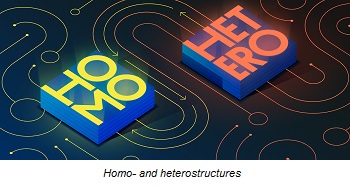
A physical effect known as superinjection underlies modern light-emitting diodes (LEDs) and lasers. For decades this effect was believed to occur only in semiconductor heterostructures — that is, structures composed of two or more semiconductor materials. Researchers from the Moscow Institute of Physics and Technology have found superinjection to be possible in homostructures, which are made of a single material. This opens up entirely new prospects for the development of light sources.
Semiconductor light sources, such as lasers and LEDs, are at the core of modern technology. They enable laser printers and high-speed internet. But a mere 60 years ago, no one would imagine semiconductors being used as materials for bright light sources. The problem was that to generate light, such devices require electrons and holes — the free charge carriers in any semiconductor — to recombine. The higher the concentration of electrons and holes, the more often they recombine, making the light source brighter. However, for a long time, no semiconductor device could be manufactured to provide a sufficiently high concentration of both electrons and holes.
The solution was found in the 1960s by Zhores Alferov and Herbert Kroemer. They proposed to use heterostructures, or “sandwich” structures, consisting of two or more complementary semiconductors instead of just one. If one places a semiconductor between two semiconductors with wider bandgaps and applies a forward bias voltage, the concentration of electrons and holes in the middle layer can reach values that are orders of magnitude higher than those in the outer layers. This effect, known as superinjection, underlies modern semiconductor lasers and LEDs. Its discovery earned Alferov and Kroemer the Nobel Prize in physics in 2000.
However, two arbitrary semiconductors cannot make a viable heterostructure. The semiconductors need to have the same period of the crystal lattice. Otherwise, the number of defects at the interface between the two materials will be too high, and no light will be generated. In a way, this would be similar to trying to screw a nut on a bolt whose thread pitch does not match that of the nut. Since homostructures are composed of just one material, one part of the device is a natural extension of the other. Although homostructures are easier to fabricate, it was believed that homostructures could not support superinjection and therefore are not a viable basis for practical light sources.
Igor Khramtsov and Dmitry Fedyanin from the Moscow Institute of Physics and Technology made a discovery that drastically changes the perspective on how light-emitting devices can be designed. The physicists found that it is possible to achieve superinjection with just one material. What is more, most of the known semiconductors can be used.
“In the case of silicon and germanium, superinjection requires cryogenic temperatures, and this casts doubt on the utility of the effect. But in diamond or gallium nitride, strong superinjection can occur even at room temperature,” Dr. Fedyanin said. This means that the effect can be used to create mass market devices. According to the new paper, superinjection can produce electron concentrations in a diamond diode that are 10,000 times higher than those previously believed to be ultimately possible. As a result, diamond can serve as the basis for ultraviolet LEDs thousands of times brighter than what the most optimistic theoretical calculations predicted. “Surprisingly, the effect of superinjection in diamond is 50 to 100 times stronger than that used in most mass market semiconductor LEDs and lasers based on heterostructures,” Khramtsov pointed out.
The physicists emphasized that superinjection should be possible in a wide range of semiconductors, from conventional wide-bandgap semiconductors to novel two-dimensional materials. This opens up new prospects for designing highly efficient blue, violet, ultraviolet, and white LEDs, as well as light sources for optical wireless communication (Li-Fi), new types of lasers, transmitters for the quantum internet, and optical devices for early disease diagnostics.
Share on:


Testimonial
"The I-Connect007 team is outstanding—kind, responsive, and a true marketing partner. Their design team created fresh, eye-catching ads, and their editorial support polished our content to let our brand shine. Thank you all! "
Sweeney Ng - CEE PCBSuggested Items
Fresh PCB Concepts: Designing for Success at the Rigid-flex Transition Area
08/28/2025 | Team NCAB -- Column: Fresh PCB ConceptsRigid-flex PCBs come in all shapes and sizes. Manufacturers typically use fire-retardant, grade 4 (FR-4) materials in the rigid section and flexible polyimide materials in the flex region. Because of the small size, some rigid-flex PCBs, like those for hearing aid devices, are among the most challenging to manufacture. However, regardless of its size, we should not neglect the transition area between the rigid and flexible material.
Global Sourcing Spotlight: How to Evaluate Supplier Capabilities Worldwide
08/20/2025 | Bob Duke -- Column: Global Sourcing SpotlightIn global sourcing, the difference between a competitive edge and a catastrophic disruption often comes down to how well you vet your suppliers. Sourcing advanced PCBs, precision components, or materials for complex assemblies demands diligence, skepticism, and more than a little time on airplanes. Here’s how to do your due diligence when evaluating international suppliers and why cutting corners can cost you more than money.
Insulectro and Electroninks Sign North American Distribution Agreement
08/12/2025 | InsulectroElectroninks, a leader in metal organic decomposition (MOD) inks for additive manufacturing and advanced semiconductor packaging, today announced a strategic collaboration and distribution partnership with Insulectro, a premier distributor of materials used in printed electronics and advanced interconnect manufacturing.
Happy’s Tech Talk #41: Sustainability and Circularity for Electronics Manufacturing
08/13/2025 | Happy Holden -- Column: Happy’s Tech TalkI attended INEMI’s June 12 online seminar, “Sustainable Electronics Tech Topic Series: PCBs and Sustainability.” Dr. Maarten Cauwe of imec spoke on “Life Cycle Inventory (LCI) Models for Assessing and Improving the Environmental Impact of PCB Assemblies,” and Jack Herring of Jiva Materials Ltd. spoke on “Transforming Electronics with Recyclable PCB Technology.” This column will review information and provide analysis from both presentations.
Dymax Renews Connecticut Headquarters Lease, Reinforces Long-Term Commitment to Local Community
08/08/2025 | DymaxDymax, a global manufacturer of rapid light-curing materials and equipment, is pleased to announce the renewal and extension of its corporate lease at its 318 Industrial Lane, Torrington, headquarters.