


 Dan’s Biz Bookshelf: ‘Abundance: How We Build a Better Future’
 Trouble in Your Tank: In Complex Systems, Design Rules Aren’t Optional
 It’s Only Common Sense: The Phone Is Still Your Competitive Advantage


Scientists 3D-Print All-Liquid ‘Lab on a Chip’
April 29, 2019 | Berkeley LabEstimated reading time: 3 minutes
Researchers at DOE’s Lawrence Berkeley National Laboratory (Berkeley Lab) have 3D-printed an all-liquid device that, with the click of a button, can be repeatedly reconfigured on demand to serve a wide range of applications—from making battery materials to screening drug candidates.
“What we demonstrated is remarkable. Our 3D-printed device can be programmed to carry out multistep, complex chemical reactions on demand,” said Brett Helms, a staff scientist in Berkeley Lab’s Materials Sciences Division and Molecular Foundry, who led the study. “What’s even more amazing is that this versatile platform can be reconfigured to efficiently and precisely combine molecules to form very specific products, such as organic battery materials.”
The study’s findings, which were reported in the journal Nature Communications, is the latest in a series of experiments at Berkeley Lab that fabricate all-liquid materials with a 3D printer.
Last year, a study co-authored by Helms and Thomas Russell, a visiting researcher from the University of Massachusetts at Amherst who leads the Adaptive Interfacial Assemblies Toward Structured Liquids Program in Berkeley Lab’s Materials Sciences Division, pioneered a new technique for printing various liquid structures—from droplets to swirling threads of liquid—within another liquid.
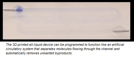
Image Caption: When two liquids—one containing nanoscale clay particles, another containing polymer particles—are printed onto a glass substrate, they come together at the interface of the two liquids and within milliseconds form a very thin channel or tube about 1 millimeter in diameter.
“After that successful demonstration, a bunch of us got together to brainstorm on how we could use liquid printing to fabricate a functioning device,” said Helms. “Then it occurred to us: If we can print liquids in defined channels and flow contents through them without destroying them, then we could make useful fluidic devices for a wide range of applications, from new types of miniaturized chemical laboratories to even batteries and electronic devices.”
To make the 3D-printable fluidic device, lead author Wenqian Feng, a postdoctoral researcher in Berkeley Lab’s Materials Sciences Division, designed a specially patterned glass substrate. When two liquids—one containing nanoscale clay particles, another containing polymer particles—are printed onto the substrate, they come together at the interface of the two liquids and within milliseconds form a very thin channel or tube about 1 millimeter in diameter.
Once the channels are formed, catalysts can be placed in different channels of the device. The user can then 3D-print bridges between channels, connecting them so that a chemical flowing through them encounters catalysts in a specific order, setting off a cascade of chemical reactions to make specific chemical compounds. And when controlled by a computer, this complex process can be automated “to execute tasks associated with catalyst placement, build liquid bridges within the device, and run reaction sequences needed to make molecules,” said Russell.
Page 1 of 2
Share on:


Subscribe
Stay ahead of the technologies shaping the future of electronics with our latest newsletter, Advanced Electronics Packaging Digest. Get expert insights on advanced packaging, materials, and system-level innovation, delivered straight to your inbox.
Subscribe now to stay informed, competitive, and connected.
Suggested Items
AI Demand Drives PCB Material Market Growth
05/08/2026 | TPCAAs AI computing continues to drive a comprehensive upgrade in hardware specifications, the global printed circuit board industry is undergoing a profound structural transformation.
I-Connect007 Editor’s Choice: Five Must-Reads for the Week
05/01/2026 | Michelle Te, I-Connect007If it feels like the PCB industry is accelerating faster than ever, you’re not imagining it. From advanced materials driven by AI applications to renewed investment in domestic manufacturing—and the next generation stepping into critical roles—there’s a lot shifting at once. My selections for this week highlight where the pressure points are forming, and where the opportunities are emerging.
Electronics Manufacturing Needs Your Voice: Global Sentiment Survey Now Live
04/30/2026 | Global Electronics AssociationThe latest monthly Global Sentiment Survey from the Global Electronics Association is now open. At a time when demand uncertainty, policy shifts, energy costs, and supply chain recalibration are pulling the industry in multiple directions, the survey captures something macroeconomic data often misses: how manufacturers are actually experiencing conditions on the ground.
From Backbone to Breakthroughs: I-Connect007 Wraps PCB Materials Series with Focus on Innovation
05/06/2026 | I-Connect007I-Connect007 wraps up its six-part podcast series, PCB Materials: The Backbone and Future of Electronics, with Episode 6 and a discussion focusing on innovation. In Episode 6, Marcy LaRont speaks with Isola CTO Kirk Thompson about a critical turning point for the PCB industry as innovation accelerates. As data rates climb and demands from AI infrastructure, power density, flexible electronics, photonics, and chiplet integration intensify, traditional material assumptions are no longer sufficient.
Jiva Soluboard Getting the Attention It Deserves
04/30/2026 | Marcy LaRont, I-Connect007 MagazineJiva is a newer company that bridges the divide between PCB fabrication and product circularity or sustainability. Jiva Soluboard is the first fully recyclable laminate material ever created for PCB fabrication, and it's not going unnoticed. Stephen Driver, CEO of Jiva, gave us an update at APEX EXPO, including an exciting certification achievement in February.