


 Driving Innovation: Mechanical and Optical Processes During Rigid-flex Production
 It’s Only Common Sense: Your Biggest Competitor Is Complacency
 The Chemical Connection: Onshoring PCB Production—Daunting but Certainly Possible


Water Creates Traps in Organic Electronics
May 1, 2019 | Linköping UniversityEstimated reading time: 3 minutes
Poor-quality organic semiconductors can become high-quality semiconductors when manufactured in the correct way. Researchers at Linköping University show in an article in Nature Materials that the motion of charges in organic electronic devices is dramatically slowed down by minute amounts of water.
The discovery that organic materials, such as polymers, can act as semiconductors led to a Nobel Prize in Chemistry in 2000. Since then, research within organic electronics has truly exploded, not least at Linköping University, which is home to world-leading research in the field.
Organic semiconductors, however, do not conduct current as efficiently as, for example, semiconductors of silicon or other inorganic materials. The scientists have discovered that one of the causes of this is the formation of traps in the organic materials in which the charge carriers get stuck. Several research groups around the world have been working hard to understand not only where the traps are located, but also how they can be eliminated.
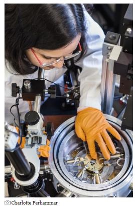
Image Caption: Tanvi Upreti är doktorand vid avdelningen Komplexa material och system har utfört de praktiska experimenten tillsammans med förste författaren Guangzheng Zuo. Tanvi Upreti, doctoral student at the Division for Complex Materials and Devices, who carried out the experiments together with the first author, Guangzheng Zuo.
Traps in Organic Semiconductors
“There are traps in all organic semiconductors, but they are probably a greater problem in n-type materials, since these are generally poorer semiconductors than p-type materials”, says Martijn Kemerink, professor of applied physics in the Division for Complex Materials and Devices at Linköping University.
Materials of p-type have a positive charge and the charge carriers consist of holes, while materials of n-type have charge carriers in the form of electrons, which gives the material a negative charge.
Martijn Kemerink and his colleagues at Linköping University have concluded that water is the villain in the piece. Specifically, the water is thought to sit in nanometre-sized pores in the organic material and is absorbed from the environment.
“In a p-type material the dipoles in the water align with their negative ends towards the holes, which are positively charged, and the energy of the complete system is lowered. You could say that the dipoles embed the charge carriers such that they cannot go anywhere anymore”, says Martijn Kemerink.
For n-type materials, the water orients the other way around, but the effect is the same, the charge is trapped.
Experiments have been carried out in which the material is heated, to dry it out and cause the water to disappear. It works fine for a while, but the material subsequently re-absorbs water from the surrounding air, and much of the benefit gained by drying disappears.
Manufacture in a Dry Atmosphere
“The more water, the more traps. We have also shown that the drier the films can be manufactured, the better conductors they are. The theoretical work by Mathieu Linares Tanvi Upreti är doktorand vid avdelningen Komplexa material och system har utfört de praktiska experimenten tillsammans med förste författaren Guangzheng Zuo. Tanvi Upreti, doctoral student at the Division for Complex Materials and Devices, who carried out the experiments together with the first author, Guangzheng Zuo.
quantitatively confirmed our ideas about what was going on, which was very satisfactory. Our article in Nature Materials shows not only how to get the water out, but also how to make sure that the water stays out, in order to produce an organic material with stable conductivity.”
In order to prevent the reuptake of water into the material once it has been dried, the scientists have also developed a way to remove the voids into which water molecules otherwise would have penetrated. This method is based on a combination of heating the material in the presence of a suitable organic solvent.
“Materials that were previously believed to be extremely poor semiconductors can instead become good semiconductors, as long as they are manufactured in a dry atmosphere. We have shown that dry-prepared materials tend to remain dry, while materials that are made in the presence of water can be dried. The latter are, however, extremely sensitive to water. This is true of the materials we have tested, but there’s nothing to suggest that other organic semiconducting materials behave differently”, says Martijn Kemerink.
Share on:


Testimonial
"We’re proud to call I-Connect007 a trusted partner. Their innovative approach and industry insight made our podcast collaboration a success by connecting us with the right audience and delivering real results."
Julia McCaffrey - NCAB GroupSuggested Items
Sealed for Survival: Potting Electronics for the Toughest Environments
10/29/2025 | Beth Massey, MacDermid Alpha Electronics SolutionsElectronics deployed in harsh conditions face relentless threats from vibration, impact, chemical contaminants, airborne pollutants, and moisture, conditions that can quickly lead to failure without robust protection. Potting, the process of encapsulating electronics in a protective polymer, is a widely used strategy to safeguard devices from both environmental and mechanical hazards.
Driving Innovation: Mechanical and Optical Processes During Rigid-flex Production
10/28/2025 | Kurt Palmer -- Column: Driving InnovationRigid-flex printed circuit boards are a highly effective solution for placing complex circuitry in tight, three-dimensional spaces. They are now indispensable across a range of industries, from medical devices and aerospace to advanced consumer electronics, helping designers make the most efficient use of available space. However, their unique construction—combining rigid and flexible materials—presents a fundamental challenge for PCB manufacturers.
SMTAI 2025 Review: Reflecting on a Pragmatic and Forward-looking Industry
10/27/2025 | Marcy LaRont, I-Connect007Leaving the show floor on the final afternoon of SMTA International last week in Rosemont, Illinois, it was clear that the show remains a grounded, technically driven event that delivers a solid program, good networking, and an easy space to commune with industry colleagues and meet with customers.
ITW EAE Despatch Ovens Now Support ASTM 5423 Testing
10/15/2025 | ITW EAEAs the demand for high-performance electrical insulation materials continues to grow—driven by the rapid expansion of electric vehicles (EVs) and energy storage systems—thermal processing has become a critical step in material development.
Beyond Thermal Conductivity: Exploring Polymer-based TIM Strategies for High-power-density Electronics
10/13/2025 | Padmanabha Shakthivelu and Nico Bruijnis, MacDermid Alpha Electronics SolutionsAs power density and thermal loads continue to increase, effective thermal management becomes increasingly important. Rapid and efficient heat transfer from power semiconductor chip packages is essential for achieving optimal performance and ensuring long-term reliability of temperature-sensitive components. This is particularly crucial in power systems that support advanced applications such as green energy generation, electric vehicles, aerospace, and defense, along with high-speed computing for data centers and artificial intelligence (AI).