


 Dan’s Biz Bookshelf: ‘Abundance: How We Build a Better Future’
 Trouble in Your Tank: In Complex Systems, Design Rules Aren’t Optional
 It’s Only Common Sense: The Phone Is Still Your Competitive Advantage


Researchers Identify New 2D Insulators with Ferromagnetic Properties
May 13, 2019 | Ames LaboratoryEstimated reading time: 2 minutes
Collaborating scientists at the U.S. Department of Energy’s Ames Laboratory, Brookhaven National Laboratory, and Princeton University have discovered a new layered ferromagnetic semiconductor, a rare type of material that holds great promise for next-generation electronic technologies.
As the name implies, semiconductors are the Goldilocks of electrically conductive materials-- not a metal, and not an insulator, but a “just-right” in-between whose conducting properties can be altered and customized in ways that create the basis for the world’s modern electronic capabilities. Especially rare are the ones closer to an insulator than to a metal.
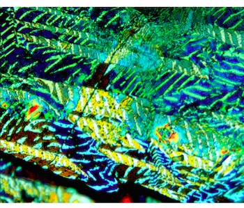
The recent discovery of ferromagnetism in semiconducting materials has been limited to a handful of mostly chromium-based compounds. But here, the researchers discovered ferromagnetism in a vanadium-iodine semiconductor, a material which has long been known but ignored; and which scientist Tai Kong compared to finding a “hidden treasure in our own backyard.” Now a postdoctoral researcher in the lab of Robert J. Cava, the Russell Wellman Moore Professor of Chemistry at Princeton University, Kong completed PhD research at the Ames Laboratory under supervision of Paul C. Canfield. And when new material could have ferromagnetic response, Kong turned to Ames Laboratory for the magneto-optical visualization of magnetic domains that serves as the definitive proof of ferromagnetism.
“Being able to exfoliate these materials down into 2D layers gives us new opportunities to find unusual properties that are potentially useful to electronic technology advances,” said Kong. “It’s sort of like getting a new shape of Lego bricks. The more unique pieces you have, the cooler the stuff you can build.”
The advantage of ferromagnetism in a semiconductor is that electronic properties become spin-dependent. Electrons align their spins along internal magnetization.
“This creates an additional control knob to manipulate currents flowing through a semiconductor by manipulating magnetization, either by changing the magnetic field or by other more complex means, while the amount of current that can be carried may be controlled by doping (adding small amount of other materials),” said Ames Laboratory Scientist Ruslan Prozorov. “These additional ways to control behavior and the potential to discover novel effects are the reason for such high interest in finding insulators and semiconductors that are also ferromagnets.”
Share on:


Subscribe
Stay ahead of the technologies shaping the future of electronics with our latest newsletter, Advanced Electronics Packaging Digest. Get expert insights on advanced packaging, materials, and system-level innovation, delivered straight to your inbox.
Subscribe now to stay informed, competitive, and connected.
Suggested Items
AI Demand Drives PCB Material Market Growth
05/08/2026 | TPCAAs AI computing continues to drive a comprehensive upgrade in hardware specifications, the global printed circuit board industry is undergoing a profound structural transformation.
I-Connect007 Editor’s Choice: Five Must-Reads for the Week
05/01/2026 | Michelle Te, I-Connect007If it feels like the PCB industry is accelerating faster than ever, you’re not imagining it. From advanced materials driven by AI applications to renewed investment in domestic manufacturing—and the next generation stepping into critical roles—there’s a lot shifting at once. My selections for this week highlight where the pressure points are forming, and where the opportunities are emerging.
Electronics Manufacturing Needs Your Voice: Global Sentiment Survey Now Live
04/30/2026 | Global Electronics AssociationThe latest monthly Global Sentiment Survey from the Global Electronics Association is now open. At a time when demand uncertainty, policy shifts, energy costs, and supply chain recalibration are pulling the industry in multiple directions, the survey captures something macroeconomic data often misses: how manufacturers are actually experiencing conditions on the ground.
From Backbone to Breakthroughs: I-Connect007 Wraps PCB Materials Series with Focus on Innovation
05/06/2026 | I-Connect007I-Connect007 wraps up its six-part podcast series, PCB Materials: The Backbone and Future of Electronics, with Episode 6 and a discussion focusing on innovation. In Episode 6, Marcy LaRont speaks with Isola CTO Kirk Thompson about a critical turning point for the PCB industry as innovation accelerates. As data rates climb and demands from AI infrastructure, power density, flexible electronics, photonics, and chiplet integration intensify, traditional material assumptions are no longer sufficient.
Jiva Soluboard Getting the Attention It Deserves
04/30/2026 | Marcy LaRont, I-Connect007 MagazineJiva is a newer company that bridges the divide between PCB fabrication and product circularity or sustainability. Jiva Soluboard is the first fully recyclable laminate material ever created for PCB fabrication, and it's not going unnoticed. Stephen Driver, CEO of Jiva, gave us an update at APEX EXPO, including an exciting certification achievement in February.