


 Dan’s Biz Bookshelf: ‘Abundance: How We Build a Better Future’
 Trouble in Your Tank: In Complex Systems, Design Rules Aren’t Optional
 It’s Only Common Sense: The Phone Is Still Your Competitive Advantage


A New Sensor for Light, Heat and Touch
May 14, 2019 | Linköping UniversityEstimated reading time: 3 minutes
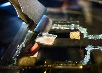
Inspired by the behaviour of natural skin, researchers at the Laboratory of Organic Electronics have developed a sensor that will be suitable for use with electronic skin. It can measure changes in body temperature, and react to both sunlight and warm touch.
Robotics, prostheses that react to touch, and health monitoring are three fields in which scientists globally are working to develop electronic skin. They want such skin to be flexible and to possess some form of sensitivity. Researchers at the Laboratory of Organic Electronics at Linköping University have now taken steps towards such a system by combining several physical phenomena and materials. The result is a sensor that, similar to human skin, can sense temperature variation that originates from the touch of a warm object, as well as the heat from solar radiation.
Mina Shiran Chaharsoughi and Magnus Jonsson
Inspiration from Nature
“We have been inspired by nature and its methods of sensing heat and radiation”, says Mina Shiran Chaharsoughi, doctoral student in the Organic Photonics and Nano-optics group at the Laboratory of Organic Electronics.
Together with colleagues she has developed a sensor that combines pyroelectric and thermoelectric effects with a nano-optical phenomenon.
A voltage arises in pyroelectric materials when they are heated or cooled. It is the change in temperature that gives a signal, which is rapid and strong, but that decays almost as rapidly.
In thermoelectric materials, in contrast, a voltage arises when the material has one cold and one hot side. The signal here arises slowly, and some time must pass before it can be measured. The heat may arise from a warm touch or from the sun; all that is required is that one side is colder than the other.
“We wanted to enjoy the best of both worlds, so we combined a pyroelectric polymer with a thermoelectric gel developed in a previous project by Dan Zhao, Simone Fabiano and other colleagues at the Laboratory of Organic Electronics. The combination gives a rapid and strong signal that lasts as long as the stimulus is present”, says Magnus Jonsson, leader of the Organic Photonics and Nano-optics group.
Furthermore, it turned out that the two materials interact in a way that reinforces the signal.
Plasmons
The new sensor also uses another nano-optical entity known as plasmons.
“Plasmons arise when light interacts with nanoparticles of metals such as gold and silver. The incident light causes the electrons in the particles to oscillate in unison, which forms the plasmon. This phenomenon provides the nanostructures with extraordinary optical properties, such as high scattering and high absorption”, Magnus Jonsson explains.
In previous work, he and his co-workers have shown that a gold electrode that has been perforated with nanoholes absorbs light efficiently with the aid of plasmons. The absorbed light is subsequently converted to heat. With such an electrode, a thin gold film with nanoholes, on the side that faces the sun, the sensor can also convert visible light rapidly to a stable signal.
As an added bonus, the sensor is also pressure-sensitive.
“A signal arises when we press the sensor with a finger, but not when we subject it to the same pressure with a piece of plastic. It reacts to the heat of the hand”, says Magnus Jonsson.
In addition to Mina Shiran Chaharsoughi and Magnus Jonsson, their colleagues Dan Zhao, Simone Fabiano and Professor Xavier Crispin at the Laboratory of Organic Electronics have also contributed to the study, the results of which have recently been published in the scientific journal Advanced Functional Materials.
The research has been financed by, among other sources, the Swedish Foundation for Strategic Research, the Swedish Research Council, the Wenner-Gren Foundations, and the Strategic Initiative in Advanced Functional Materials, AFM, at Linköping University.
Share on:


Subscribe
Stay ahead of the technologies shaping the future of electronics with our latest newsletter, Advanced Electronics Packaging Digest. Get expert insights on advanced packaging, materials, and system-level innovation, delivered straight to your inbox.
Subscribe now to stay informed, competitive, and connected.
Suggested Items
AI Demand Drives PCB Material Market Growth
05/08/2026 | TPCAAs AI computing continues to drive a comprehensive upgrade in hardware specifications, the global printed circuit board industry is undergoing a profound structural transformation.
I-Connect007 Editor’s Choice: Five Must-Reads for the Week
05/01/2026 | Michelle Te, I-Connect007If it feels like the PCB industry is accelerating faster than ever, you’re not imagining it. From advanced materials driven by AI applications to renewed investment in domestic manufacturing—and the next generation stepping into critical roles—there’s a lot shifting at once. My selections for this week highlight where the pressure points are forming, and where the opportunities are emerging.
Electronics Manufacturing Needs Your Voice: Global Sentiment Survey Now Live
04/30/2026 | Global Electronics AssociationThe latest monthly Global Sentiment Survey from the Global Electronics Association is now open. At a time when demand uncertainty, policy shifts, energy costs, and supply chain recalibration are pulling the industry in multiple directions, the survey captures something macroeconomic data often misses: how manufacturers are actually experiencing conditions on the ground.
From Backbone to Breakthroughs: I-Connect007 Wraps PCB Materials Series with Focus on Innovation
05/06/2026 | I-Connect007I-Connect007 wraps up its six-part podcast series, PCB Materials: The Backbone and Future of Electronics, with Episode 6 and a discussion focusing on innovation. In Episode 6, Marcy LaRont speaks with Isola CTO Kirk Thompson about a critical turning point for the PCB industry as innovation accelerates. As data rates climb and demands from AI infrastructure, power density, flexible electronics, photonics, and chiplet integration intensify, traditional material assumptions are no longer sufficient.
Jiva Soluboard Getting the Attention It Deserves
04/30/2026 | Marcy LaRont, I-Connect007 MagazineJiva is a newer company that bridges the divide between PCB fabrication and product circularity or sustainability. Jiva Soluboard is the first fully recyclable laminate material ever created for PCB fabrication, and it's not going unnoticed. Stephen Driver, CEO of Jiva, gave us an update at APEX EXPO, including an exciting certification achievement in February.