


 Dan’s Biz Bookshelf: ‘Abundance: How We Build a Better Future’
 Trouble in Your Tank: In Complex Systems, Design Rules Aren’t Optional
 It’s Only Common Sense: The Phone Is Still Your Competitive Advantage


A Light Matter: Understanding the Raman Dance of Solids
May 22, 2019 | Tokyo Institute of TechnologyEstimated reading time: 3 minutes
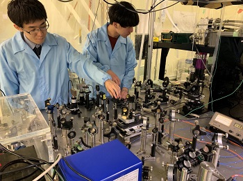
Scientists at Tokyo Institute of Technology and Keio University investigated the excitation and detection of photogenerated coherent phonons in polar semiconductor GaAs through an ultrafast dual pump-probe laser for quantum interferometry.
Imagine a world where computers can store, move, and process information at exponential speeds using what we currently term as waste vibrations--heat and noise. While this may remind us of a sci-fi movie, with the coming of the nano-age, this will very soon be reality. At the forefront of this is research in a branch of the quantum realm: quantum photonics.
Laws of physics help us understand the efficient ways of nature. However, their application to our imperfect lives often involves the most efficient ways of utilizing the laws of physics. Because most of our lives revolve around exchange of information, coming up with faster ways of communicating has always been a priority. Most of this information is encoded in the waves and vibrations that utilize electromagnetic fields that propagate in space or solids and randomly interact with the particles in solid devices, creating wasteful byproducts: heat and noise. This interaction propagates via two channels, absorption of light or scattering by light, both leading to random excitation of atoms that make up the solid. By converting this random excitation of particles into coherent, well-controlled vibrations of the solid, we can turn the tables--instead of using light, we can use sound (noise!) to transport information. The energy of this lattice vibration is packaged in well-defined bundles called phonons.
However, the scope of this relies on the understanding of two fundamental points--generation of the coherent phonons and its subsequent lifetime for which it retains its "information-transporting ability." This was the theme of the question that researchers from Nakamura's laboratory at Tokyo Institute of Technology (Tokyo Tech) sought to answer under the collaboration of Prof. Shikano, who is working at Quantum Computing Center, Keio University.
Optical phonons are used to describe a certain mode of vibration, which occurs when the neighboring atoms of the lattice move in the opposite direction. "Because impulsive absorption (IA) and impulsive stimulated Raman scattering (ISRS) cause zapping of such vibrations in the solid lattice leading to phonon creation," claims Nakamura, "our aim was to shed light on narrowing down this dichotomy." The researchers utilized dual pump-probe spectroscopy, where an ultrafast laser pulse is split into a stronger "pump" to excite the GaAs sample and a weaker "probe" beam irradiated on the "shaken" sample. The pump pulse is split into two collinear pulses but with a slight shift in their wave pattern to produce relative phase-locked pulses. The phonon amplitude is enhanced or suppressed in fringes, depending upon constructive and destructive interference (Figs. 1 and 2).
The probe beam reads the interference fringe pattern by reading off changes in optical properties (reflectivity) of the sample that arise due to the fringe pattern-dependent vibrations in the lattice. This method of reading off the changes in wave pulses to determine the sample characteristics is called quantum interferometry.
Nakamura and the team state, "Thus, by varying the time delay between the pump pulses in steps shorter than the light cycle and pump-probe pulse, we could detect the interference between electronic states as well as that of optical phonons, which shows temporal characteristics of the generation of coherent phonons via light-electron-phonon interactions during the photo excitation." From the quantum mechanical superposition, the researchers could sieve out the information: generation of the phonons was dominantly linked to scattering (ISRS).
Advances in ultrashort optical pulses generations have continually pushed the ability to probe and manipulate structural composition of materials. With the foundations laid by such studies in understanding the vibrations in solids, the next step will involve using them as building blocks for transistors, devices, electronic devices, and who knows, soon our future!
Share on:


Subscribe
Stay ahead of the technologies shaping the future of electronics with our latest newsletter, Advanced Electronics Packaging Digest. Get expert insights on advanced packaging, materials, and system-level innovation, delivered straight to your inbox.
Subscribe now to stay informed, competitive, and connected.
Suggested Items
XJTAG Launches Free Standalone ODB++ Layout Viewer for Fast PCB Signal Navigation
04/28/2026 | XJTAGXJTAG®, a trusted name in electronics testing and programming, announced the release of a free standalone Layout Viewer, designed to help engineers quickly view PCB designs using ODB++ data without requiring access to full CAD systems or test environments.
ASMPT Enhances WORKS Monitoring to Boost SMT Production Transparency and Accuracy
04/15/2026 | ASMPTASMPT SMT Solutions, the technology and market leader in integrated hardware and software solutions for electronics manufacturing, presents a new version of WORKS Monitoring.
CACI’s Spectral Program with the U.S. Navy Achieves Milestone C
03/02/2026 | CACI International Inc.CACI International Inc announced the Spectral program has successfully completed rigorous review by the U.S. Navy’s Program Executive Office for Command, Control, Communications, Computers, and Intelligence (PEO C4I), achieving Milestone C.
DesignCon Taps NASA, Purdue, and Agentrys for Keynote Slate
02/24/2026 | GlobeNewswireDesignCon, the premiere event for the latest in high-speed design tools, technologies, and developments, has announced the keynote speakers for the 2026 edition.
Zuken Automating Wire Harness Design Tools
01/28/2026 | Nolan Johnson, SMT007 MagazineHistorically, wire harness manufacturing has not been a particularly digital business model, but that is changing. Zuken USA, a stalwart in CAD tools, has recently announced multiple new tools in the wire harness space. In a conversation with Zuken’s Paul Harvell, vice president of engineering, and Geoffrey (Geo) Ng, technical marketing manager, we get details on how Zuken is helping wire harness design and manufacturing catch up and, in some ways, leapfrog the current state of the art in EMS digitization and automation.