


 The Marketing Minute: Marketing With Layers
 The Right Approach: Electro-Tek—A Williams Family Legacy, Part 1
 It’s Only Common Sense: If You’re Not Differentiated, You’re Dead


DGIST Develops Next Generation Core Semiconductor Technology
May 24, 2019 | DGISTEstimated reading time: 2 minutes
The DGIST Department of Information and Communication Engineering developed a graphene-based high-performance transmission line with an improved operating speed of electrons than using the existing metal in high-frequency. This is expected to contribute greatly to next generation’s high-speed semiconductor and communication device with much faster processing speed than the existing one.
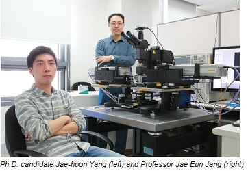
DGIST announced on Thursday, May 2 that Professor Jae Eun Jang’s team researched the high frequency transmission characteristics of single-layer graphene in the Department of Information and Communication Engineering, and developed a high-performance, high-frequency transmission line that induced an increase of device concentration inside graphene. This result showed the characteristics of high frequency transmission with great improvement that can replace the metal used in the existing high-speed semiconductor processing, and its potential use as a transmission line of graphene is expected in the future.
Due to the high-integration and high speed of semiconductor devices, the resistance of metal wire in which signals among devices are transmitted has increased geometrically, reaching the limit of permissible current density. To resolve this issue, carbon-based nano structures such as graphene and carbon nano tube, which are regarded as the substitutes of existing metals, have drawn attention as next generation new materials.
However, graphene has a hexagonal array of carbon, with very thin thickness of 0.3nm, electric conductivity that is 100 times greater than copper, and electron mobility that is 100 times faster than silicon. It has thus been mentioned as an electronic material that can replace the existing metal and semiconductor materials. However, pure graphene has too low device concentration of 1012 cm-2 with thin structural characteristics of nanometer, which results in too high resistance of graphene.
In order to overcome such limitations, Professor Jang’s team conducted a research to improve high frequency transmission characteristics of graphene by enhancing the device concentration inside graphene. By combining graphene and amorphous carbon, the team increased the device concentration of graphene and enhanced the electrical characteristics of graphene. The high frequency transmission of increased graphene was –8dB, which could be comparable to metal nano lines with hundreds of nano size.
The team also proved that defects inside graphene decrease the high frequency transmission of graphene and developed a new, stable doping technique that minimized internal defects. This new doping technique increased the device concentration of graphene by 2x 1013cm-2 and showed stable thermal properties and electrical characteristics.
The high frequency graphene transmission line developed by Professor Jang’s research team displayed high signal transmission efficiency and stable operating characteristics, which can be applied to the metal wiring processing of the existing semiconductor industry as well as next generation integrated circuit.
Professor Jae Eun Jang in the Department of Information and Communication Engineering said “Along with device technology, transmission line is a very important technology in the semiconductor research field. We have developed a core base technology that can enhance the high frequency transmission of graphene that can be used as next generation transmission line. Thanks to the results of convergence research by experts in nano engineering, electronic engineering, and physics, we expect to use the graphene on high-frequency circuit such as MMIC and RFIC.
This research was performed with the support of the Ministry of Science and ICT and basic research project of the National Research Foundation of Korea, and it has been selected to be published as a cover paper of ‘‘Advanced Functional Materials’, a worldwide international journal in material science.
Share on:


Testimonial
"In a year when every marketing dollar mattered, I chose to keep I-Connect007 in our 2025 plan. Their commitment to high-quality, insightful content aligns with Koh Young’s values and helps readers navigate a changing industry. "
Brent Fischthal - Koh YoungSuggested Items
Episode 6 of Ultra HDI Podcast Series Explores Copper-filled Microvias in Advanced PCB Design and Fabrication
10/15/2025 | I-Connect007I-Connect007 has released Episode 6 of its acclaimed On the Line with... American Standard Circuits: Ultra High Density Interconnect (UHDI) podcast series. In this episode, “Copper Filling of Vias,” host Nolan Johnson once again welcomes John Johnson, Director of Quality and Advanced Technology at American Standard Circuits, for a deep dive into the pros and cons of copper plating microvias—from both the fabricator’s and designer’s perspectives.
Nolan’s Notes: Tariffs, Technologies, and Optimization
10/01/2025 | Nolan Johnson -- Column: Nolan's NotesLast month, SMT007 Magazine spotlighted India, and boy, did we pick a good time to do so. Tariff and trade news involving India was breaking like a storm surge. The U.S. tariffs shifted India from one of the most favorable trade agreements to the least favorable. Electronics continue to be exempt for the time being, but lest you think that we’re free and clear because we manufacture electronics, steel and aluminum are specifically called out at the 50% tariff levels.
MacDermid Alpha & Graphic PLC Lead UK’s First Horizontal Electroless Copper Installation
09/30/2025 | MacDermid Alpha & Graphic PLCMacDermid Alpha Electronics Solutions, a leading supplier of integrated materials and chemistries to the electronics industry, is proud to support Graphic PLC, a Somacis company, with the installation of the first horizontal electroless copper metallization process in the UK.
Electrodeposited Copper Foils Market to Grow by $11.7 Billion Over 2025-2032
09/18/2025 | Globe NewswireThe global electrodeposited copper foils market is poised for dynamic growth, driven by the rising adoption in advanced electronics and renewable energy storage solutions.
MacDermid Alpha Showcases Advanced Interconnect Solutions at PCIM Asia 2025
09/18/2025 | MacDermid Alpha Electronics SolutionsMacDermid Alpha Electronic Solutions, a global leader in materials for power electronics and semiconductor assembly, will showcase its latest interconnect innovations in electronic interconnect materials at PCIM Asia 2025, held from September 24 to 26 at the Shanghai New International Expo Centre, Booth N5-E30