


 Dan’s Biz Bookshelf: ‘Abundance: How We Build a Better Future’
 Trouble in Your Tank: In Complex Systems, Design Rules Aren’t Optional
 It’s Only Common Sense: The Phone Is Still Your Competitive Advantage


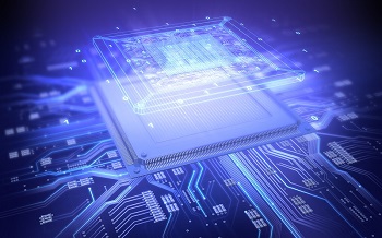
Towards Thinner and Faster Transistors
May 28, 2019 | A*STAREstimated reading time: 2 minutes
Nanoribbon field effect transistors could usher in the next generation of computing.
At the heart of every computer and smartphone, billions of microscopic silicon transistors etched into a tiny chip perform digital calculations at mind-boggling speeds. A transistor turns on or off the current flowing through it, depending on the input voltage it receives. Smaller transistors require only small voltages and can switch between states quickly, leading to increased performance.
The continued shrinking of silicon transistors has made computers faster, cheaper and more efficient over time, with Moore’s Law predicting that twice as many transistors can be fitted into an integrated circuit every two years. “However, in the past decade, silicon transistors have become so small that their performance has degraded due to quantum effects,” said Dharmraj Subhash Kotekar-Patil, a researcher at A*STAR’s Institute of Materials Research and Engineering (IMRE).
Seeking to overcome these limitations, Kotekar-Patil and colleagues are exploring new materials to create the next generation of smaller, faster transistors. They focused their efforts on molybdenum disulphide (MoS2), a transition metal dichalcogenide that is known to exhibit interesting electrical properties such as high charge mobility, high on/off ratio and low contact resistance.
In this study, the researchers optimized the stepwise process needed to manufacture nanoribbons of MoS2 at high resolution—down to 50 nanometers—to produce field effect transistors (FETs), devices that direct current flow using an electric field.
“Previous work focused on MoS2 nanoribbon FETs that are about 6 to 11 nanometers thick. We have now demonstrated the first nanoribbon FET in single layer MoS2 that is only 0.7 nanometers thick, with FET properties outperforming previous reports,” Kotekar-Patil said.
For instance, in terms of mobility, which is the measure of how fast charge carriers move in a material system, the team’s nanoribbon FET displayed almost double the mobility of existing devices. The researchers also reported transistor switching speeds that are almost three times faster than earlier systems. Nonetheless, more research is required to grow and etch single layer MoS2 FETs across an entire semiconductor wafer before the process can be carried out at an industrially relevant scale.
“Commercializing these smaller, faster transistors would result in significant increases in the performance of computer processors,” said Kotekar-Patil. “In addition, MoS2nanoribbon transistors could be used to trap single electrons and use their spin properties to encode information for quantum computing, which is an ongoing and active area of research at IMRE.”
Share on:


Subscribe
Stay ahead of the technologies shaping the future of electronics with our latest newsletter, Advanced Electronics Packaging Digest. Get expert insights on advanced packaging, materials, and system-level innovation, delivered straight to your inbox.
Subscribe now to stay informed, competitive, and connected.
Suggested Items
Zhen Ding, Tsinghua University Launch Phase II R&D and Digital Transformation Program
04/30/2026 | Zhen DingZhen Ding Technology Holding Limited, a global leader in the PCB industry, held the launch ceremony for the Phase II (2026-2030) Industry-Academia Collaboration Program of the Zhen Ding-Tsinghua Joint Research Center at the Zhen Ding Technology Lecture Hall on the Tsinghua University campus.
AT&S Advances Glass Core Substrates for AI, HPC, and Photonics
04/22/2026 | AT&SAT&S is advancing glass core substrates from research toward industrial use in artificial intelligence, high-performance computing, high-speed communications and photonics.
IBM, UIUC Expand Discovery Accelerator for AI and Quantum Computing
04/20/2026 | PRNewswireIBM and the Grainger College of Engineering at the University of Illinois Urbana-Champaign (U. of I.) announced an expansion of the IBM-Illinois Discovery Accelerator Institute.
Long Night of Research 2026: AT&S Brings Artificial Intelligence to Life
04/15/2026 | AT&SWhen the Long Night of Research takes place throughout Austria on Friday, April 24, setting an example for the country’s innovative strength, AT&S will be there with a special highlight.
Foxconn Recognized as Top 100 Global Innovators 2026
04/14/2026 | FoxconnHon Hai Technology Group (Foxconn) has been named in Clarivate’s Top 100 Global Innovators 2026, a milestone for the ninth year running and as the accelerating role of artificial intelligence stood out in innovation activity among peers in the prestigious ranking.