


 Dan’s Biz Bookshelf: ‘Abundance: How We Build a Better Future’
 Trouble in Your Tank: In Complex Systems, Design Rules Aren’t Optional
 It’s Only Common Sense: The Phone Is Still Your Competitive Advantage


Quantum Information Gets a Boost from Thin-Film Breakthrough
May 30, 2019 | Los Alamos National LaboratoryEstimated reading time: 2 minutes
Efforts to create reliable light-based quantum computing, quantum key distribution for cybersecurity, and other technologies got a boost from a new study demonstrating an innovative method for creating thin films to control the emission of single photons.
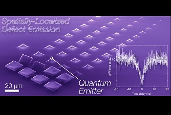
Image Caption: An innovative method for controlling single-photon emission for specific locations in 2D materials may offer a new path toward all-optical quantum computers and other quantum technologies. This image shows a false-color scanning electron micrograph of the array used to create place single-photon sources in epitaxial tungsten diselenide. Inset shows the Hanbury-Brown Twiss interferometry measurement proving quantum emission.
“Efficiently controlling certain thin-film materials so they emit single photons at precise locations—what’s known as deterministic quantum emission—paves the way for beyond-lab-scale quantum materials,” said Michael Pettes, a Los Alamos National Laboratory materials scientist and leader of the multi-institution research team.
The scalability of these two-dimensional, tungsten/selenium thin films makes them potentially useful in processes to manufacture quantum technologies. Single-photon generation is a requirement for all-optical quantum computing and key distribution in quantum communications, and it is crucial for advancing quantum information technologies.
The project, documented as a Featured Article in the journal Applied Physics Letters this week, exploits strain at highly spatially localized and well-separated emission sites, or tips, in a tungsten/selenium film. The team synthesized the film through chemical vapor deposition using a multi-step, diffusion-mediated gas source.
Because the material is very thin, it conforms to the radius of the tips and the material bends towards the substrate by more than a few percent, like someone lying on a bed of nails. The resulting strain is enough to change the electronic structure, but only at the tips. The affected area emits light of a different color and nature than light from the rest of the film.
“While more research is needed to fully understand the role of mechanical deformation in creating these quantum emission sites, we may enable a route to control quantum optical properties by using strain,” Pettes said. “These single-photon sources form the basis for photonics-based, all-optical quantum computing schemes.”
Engineering of quantum emission in 2D materials is still in a very early stage, the authors note. While studies have observed single photons originating from defect structures in these materials, previous work has suggested that non-uniform strain fields might govern the effect. However, the mechanism responsible for this emergent phenomenon remains unclear and is the focus of ongoing work at Los Alamos.
Share on:


Subscribe
Stay ahead of the technologies shaping the future of electronics with our latest newsletter, Advanced Electronics Packaging Digest. Get expert insights on advanced packaging, materials, and system-level innovation, delivered straight to your inbox.
Subscribe now to stay informed, competitive, and connected.
Suggested Items
AI Demand Drives PCB Material Market Growth
05/08/2026 | TPCAAs AI computing continues to drive a comprehensive upgrade in hardware specifications, the global printed circuit board industry is undergoing a profound structural transformation.
I-Connect007 Editor’s Choice: Five Must-Reads for the Week
05/01/2026 | Michelle Te, I-Connect007If it feels like the PCB industry is accelerating faster than ever, you’re not imagining it. From advanced materials driven by AI applications to renewed investment in domestic manufacturing—and the next generation stepping into critical roles—there’s a lot shifting at once. My selections for this week highlight where the pressure points are forming, and where the opportunities are emerging.
Electronics Manufacturing Needs Your Voice: Global Sentiment Survey Now Live
04/30/2026 | Global Electronics AssociationThe latest monthly Global Sentiment Survey from the Global Electronics Association is now open. At a time when demand uncertainty, policy shifts, energy costs, and supply chain recalibration are pulling the industry in multiple directions, the survey captures something macroeconomic data often misses: how manufacturers are actually experiencing conditions on the ground.
From Backbone to Breakthroughs: I-Connect007 Wraps PCB Materials Series with Focus on Innovation
05/06/2026 | I-Connect007I-Connect007 wraps up its six-part podcast series, PCB Materials: The Backbone and Future of Electronics, with Episode 6 and a discussion focusing on innovation. In Episode 6, Marcy LaRont speaks with Isola CTO Kirk Thompson about a critical turning point for the PCB industry as innovation accelerates. As data rates climb and demands from AI infrastructure, power density, flexible electronics, photonics, and chiplet integration intensify, traditional material assumptions are no longer sufficient.
Jiva Soluboard Getting the Attention It Deserves
04/30/2026 | Marcy LaRont, I-Connect007 MagazineJiva is a newer company that bridges the divide between PCB fabrication and product circularity or sustainability. Jiva Soluboard is the first fully recyclable laminate material ever created for PCB fabrication, and it's not going unnoticed. Stephen Driver, CEO of Jiva, gave us an update at APEX EXPO, including an exciting certification achievement in February.