


 Dan’s Biz Bookshelf: ‘Abundance: How We Build a Better Future’
 Trouble in Your Tank: In Complex Systems, Design Rules Aren’t Optional
 It’s Only Common Sense: The Phone Is Still Your Competitive Advantage


Laser Technique Could Unlock Use of Tough Material for Next-Generation Electronics
May 31, 2019 | Purdue UniversityEstimated reading time: 2 minutes
In 2004, researchers discovered a super thin material that is at least a 100 times stronger than steel and the best known conductor of heat and electricity.
This means that the material, graphene, could bring faster electronics than is possible today with silicon.
But to truly be useful, graphene would need to carry an electric current that switches on and off, like what silicon does in the form of billions of transistors on a computer chip. This switching creates strings of 0s and 1s that a computer uses for processing information.
Purdue University researchers, in collaboration with the University of Michigan and the Huazhong University of Science and Technology, show how a laser technique could permanently stress graphene into having a structure that allows the flow of electric current.
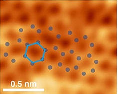
Image Caption: Graphene, a super tough wonder material, hasn’t made it into electronics yet because it doesn’t conduct an electric current on its own. Researchers used a laser technique to permanently stress graphene into a structure that allows the flow of electric current. (Purdue University image/Gary Cheng)
This structure is a so-called “band gap.” Electrons need to jump across this gap in order to become conduction electrons, which makes them capable of carrying electric current. But graphene doesn’t naturally have a band gap.
Purdue researchers created and widened the band gap in graphene to a record 2.1 electronvolts. To function as a semiconductor such as silicon, the band gap would need to be at least the previous record of 0.5 electronvolts.
“This is the first time that an effort has achieved such high band gaps without affecting graphene itself, such as through chemical doping. We have purely strained the material,” said Gary Cheng, professor of industrial engineering at Purdue, whose lab has investigated various ways to make graphene more useful for commercial applications.
The presence of a band gap allows semiconductor materials to switch between insulating or conducting an electric current, depending on whether their electrons are pushed across the band gap or not.
Surpassing 0.5 electronvolts unlocks even more potential for graphene in next-generation electronic devices, the researchers say. Their work appears in an issue of Advanced Materials.
“Researchers in the past opened the band gap by simply stretching graphene, but stretching alone doesn’t widen the band gap very much. You need to permanently change the shape of graphene to keep the band gap open,” Cheng said.
Cheng and his collaborators not only kept the band gap open in graphene, but also made it to where the gap width could be tuned from zero to 2.1 electronvolts, giving scientists and manufacturers the option to just use certain properties of graphene depending on what they want the material to do.
The researchers made the band gap structure permanent in graphene using a technique called laser shock imprinting, which Cheng developed in 2014 along with scientists at Harvard University, the Madrid Institute for Advanced Studies and the University of California, San Diego.
For this study, the researchers used a laser to create shockwave impulses that penetrated an underlying sheet of graphene. The laser shock strains graphene onto a trench-like mold – permanently shaping it. Adjusting the laser power adjusts the band gap.
While still far from putting graphene into semiconducting devices, the technique grants more flexibility in taking advantage of the material’s optical, magnetic and thermal properties, Cheng said.
The work was supported by multiple entities, including the National Science Foundation (Grant numbers CMMI-0547636 and CMMI 0928752) and the National Research Council Senior Research Associateship.
Share on:


Subscribe
Stay ahead of the technologies shaping the future of electronics with our latest newsletter, Advanced Electronics Packaging Digest. Get expert insights on advanced packaging, materials, and system-level innovation, delivered straight to your inbox.
Subscribe now to stay informed, competitive, and connected.
Suggested Items
Swinburne University, Siemens Launch Australia’s First Quantum Timing Study for Smarter Power Grids
04/30/2026 | SiemensSwinburne University of Technology and Siemens are undertaking first-of-its-kind research in Australia, into how quantum-enhanced timing can help future-proof the energy grid and increase grid stability.
Zhen Ding, Tsinghua University Launch Phase II R&D and Digital Transformation Program
04/30/2026 | Zhen DingZhen Ding Technology Holding Limited, a global leader in the PCB industry, held the launch ceremony for the Phase II (2026-2030) Industry-Academia Collaboration Program of the Zhen Ding-Tsinghua Joint Research Center at the Zhen Ding Technology Lecture Hall on the Tsinghua University campus.
IBM, UIUC Expand Discovery Accelerator for AI and Quantum Computing
04/20/2026 | PRNewswireIBM and the Grainger College of Engineering at the University of Illinois Urbana-Champaign (U. of I.) announced an expansion of the IBM-Illinois Discovery Accelerator Institute.
Honeywell, Boeing and University of Reading to Advance Aircraft-Based Sensing for Contrails
03/23/2026 | HoneywellHoneywell is collaborating with Boeing and the University of Reading on a project funded by the Aerospace Technology Institute (ATI) Programme to develop an aircraft-based prototype sensor designed to improve the understanding and mitigation of climate impacts from aircraft creating contrails.
New Research Group: AT&S Strengthens Microelectronics at TU Graz
02/11/2026 | AT&SAT&S is setting another strategic milestone for the technological future of Europe and is funding the establishment of a new research group at Graz University of Technology (TU Graz) in the field of microelectronics with a focus on IC substrates and advanced packaging technologies.