


 Dan’s Biz Bookshelf: ‘Abundance: How We Build a Better Future’
 Trouble in Your Tank: In Complex Systems, Design Rules Aren’t Optional
 It’s Only Common Sense: The Phone Is Still Your Competitive Advantage


2D Crystals Conforming to 3D Curves Create Strain for Engineering Quantum Devices
June 4, 2019 | ORNLEstimated reading time: 4 minutes
A team led by scientists at the Department of Energy’s Oak Ridge National Laboratory explored how atomically thin two-dimensional (2D) crystals can grow over 3D objects and how the curvature of those objects can stretch and strain the crystals. The findings, publishedin Science Advances, point to a strategy for engineering strain directly during the growth of atomically thin crystals to fabricate single photon emitters for quantum information processing.
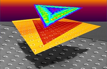
Image Caption: Strain-tolerant, triangular, monolayer crystals of WS2 were grown on SiO2 substrates patterned with donut-shaped pillars, as shown in scanning electron microscope (bottom) and atomic force microscope (middle) image elements. The curvature of the pillars induced strain in the overlying crystals that locally altered their optoelectronic properties, as shown in bright regions of photoluminescence (top). Credit: Christopher Rouleau/Oak Ridge National Laboratory, U.S. Dept. of Energy
The team first explored growth of the flat crystals on substrates patterned with sharp steps and trenches. Surprisingly, the crystals conformally grew up and down these flat obstacles without changing their properties or growth rates. However, curvy surfaces required the crystals to stretch as they grew to maintain their crystal structure. This growth of 2D crystals into the third dimension presented a fascinating opportunity.
“You can engineer how much strain you impart to a crystal by designing objects for them to grow over,” said Kai Xiao, who with ORNL colleagues David Geohegan and postdoctoral researcher Kai Wang (now at Intel) conceived the study. “Strain is one way to make ‘hot spots’ for single photon emitters.”
Conformal growth of perfect 2D crystals over 3D objects has the promise to localize strain to create high-fidelity arrays of single photon emitters. Stretching or compressing the crystal lattice changes the material’s band gap, the energy gap between the valence and conduction bands of electrons, which largely determines a material’s optoelectronic properties. Using strain engineering, researchers can funnel charge carriers to recombine precisely where desired in the crystal instead of at random defect locations. By tailoring curved objects to localize strain in the crystal, and then measuring resulting shifts in optical properties, the experimentalists compelled co-authors at Rice University—theorists Henry Yu, Nitant Gupta and Boris Yakobson—to simulate and map how curvature induces strain during crystal growth.
At ORNL, Wang and Xiao designed experiments with Bernadeta Srijanto to explore the growth of 2D crystals over lithographically patterned arrays of nanoscale shapes. Srijanto first used photolithography masks to protect certain areas of a silicon oxide surface during exposure to light, and then etched away the exposed surfaces to leave vertically standingshapes, including donuts, cones and steps. Wang and another postdoctoral researcher, Xufan Li (now at Honda Research Institute), then inserted the substrates into a furnace where vaporized tungsten oxide and sulfur reacted to deposit tungsten disulfide on the substrates as monolayer crystals. The crystals grew as an orderly lattice of atoms in perfect triangular tiles that grew larger with time by adding row after row of atoms to their outer edges. While the 2D crystals seemed to effortlessly fold like paper over tall steps and sharp trenches, growth over curved objects forced the crystals to stretch to maintain their triangular shape.
The scientists found that “donuts” 40 nanometers high were great candidates for single photon emitters because the crystals could reliably tolerate the strain they induced, and the maximum strain was precisely in the “hole” of the donut, as measured by shifts in the photoluminescence and Raman scattering. In the future, arrays of donuts or other structures could be patterned anywhere that quantum emitters are desired before the crystals are grown.
Wang and ORNL co-author Alex Puretzky used photoluminescence mapping to reveal where the crystals nucleated and how fast each edge of the triangular crystal progressed as it grew over the donuts. After careful analysis of the images, they were surprised to discover that although the crystals maintained their perfect shapes, the edges of crystals that had been strained by donuts grew faster.
To explain this acceleration, Puretzky developed a crystal growth model, and colleague Mina Yoon conducted first-principles calculations. Their work showed that strain is more likely to induce defects on the growing edge of a crystal. These defects can multiply the number of nucleation sites that seed crystal growth along an edge, allowing it to grow faster than before.
The reason crystals can grow easily up and down deep trenches, but become strained by shallow donuts, has to do with conformity and curvature. Imagine wrapping presents. Boxes are easy to wrap because the paper can fold to conform to the shape. But an irregularly shaped object with curves, such as an unboxed mug, is impossible to wrap conformally (to avoid tearing the paper, you would have to be able to stretch it like plastic wrap.)
The 2D crystals also stretch to conform to the substrate’s curves. Eventually, however, the strain becomes too great and the crystals split to release the strain, atomic force microscopy and other techniques revealed. After the crystal cracks, growth of the still-strained material proceeds in different directions for each new arm. At Nanjing University of Aeronautics and Astronautics, Zhili Hu performed phase-field simulations of crystal branching. Xiang Gao of ORNL and Mengkun Tian (formerly of the University of Tennessee) analyzed the atomic structure of the crystals by scanning transmission electron microscopy.
“The results present exciting opportunities to take two-dimensional materials and vertically integrate them into the third dimension for next-generation electronics,” said Xiao.
Next the researchers will explore whether strain can enhance the performance of tailored materials. “We’re exploring how the strain of the crystal can make it easier to induce a phase change so the crystal can take on entirely new properties,” Xiao said. “At the Center for Nanophase Materials Sciences, we’re developing tools that will allow us to probe these structures and their quantum information aspects.”
Share on:


Subscribe
Stay ahead of the technologies shaping the future of electronics with our latest newsletter, Advanced Electronics Packaging Digest. Get expert insights on advanced packaging, materials, and system-level innovation, delivered straight to your inbox.
Subscribe now to stay informed, competitive, and connected.
Suggested Items
AI Demand Drives PCB Material Market Growth
05/08/2026 | TPCAAs AI computing continues to drive a comprehensive upgrade in hardware specifications, the global printed circuit board industry is undergoing a profound structural transformation.
I-Connect007 Editor’s Choice: Five Must-Reads for the Week
05/01/2026 | Michelle Te, I-Connect007If it feels like the PCB industry is accelerating faster than ever, you’re not imagining it. From advanced materials driven by AI applications to renewed investment in domestic manufacturing—and the next generation stepping into critical roles—there’s a lot shifting at once. My selections for this week highlight where the pressure points are forming, and where the opportunities are emerging.
Electronics Manufacturing Needs Your Voice: Global Sentiment Survey Now Live
04/30/2026 | Global Electronics AssociationThe latest monthly Global Sentiment Survey from the Global Electronics Association is now open. At a time when demand uncertainty, policy shifts, energy costs, and supply chain recalibration are pulling the industry in multiple directions, the survey captures something macroeconomic data often misses: how manufacturers are actually experiencing conditions on the ground.
From Backbone to Breakthroughs: I-Connect007 Wraps PCB Materials Series with Focus on Innovation
05/06/2026 | I-Connect007I-Connect007 wraps up its six-part podcast series, PCB Materials: The Backbone and Future of Electronics, with Episode 6 and a discussion focusing on innovation. In Episode 6, Marcy LaRont speaks with Isola CTO Kirk Thompson about a critical turning point for the PCB industry as innovation accelerates. As data rates climb and demands from AI infrastructure, power density, flexible electronics, photonics, and chiplet integration intensify, traditional material assumptions are no longer sufficient.
Jiva Soluboard Getting the Attention It Deserves
04/30/2026 | Marcy LaRont, I-Connect007 MagazineJiva is a newer company that bridges the divide between PCB fabrication and product circularity or sustainability. Jiva Soluboard is the first fully recyclable laminate material ever created for PCB fabrication, and it's not going unnoticed. Stephen Driver, CEO of Jiva, gave us an update at APEX EXPO, including an exciting certification achievement in February.