


 Dan’s Biz Bookshelf: ‘Abundance: How We Build a Better Future’
 Trouble in Your Tank: In Complex Systems, Design Rules Aren’t Optional
 It’s Only Common Sense: The Phone Is Still Your Competitive Advantage


Scientists Create New Class of Two-Dimensional Materials
June 10, 2019 | University of California, IrvineEstimated reading time: 2 minutes
In a paper published this week in Nature, materials science researchers at the University of California, Irvine and other institutions unveil a new process for producing oxide perovskite crystals in exquisitely flexible, free-standing layers.
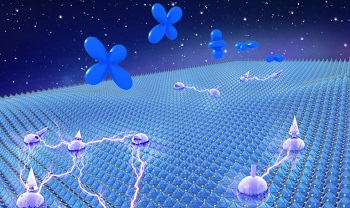
Image Caption: “Through our successful fabrication of ultrathin perovskite oxides down to the monolayer limit, we’ve created a new class of two-dimensional materials,” says Xiaoqing Pan, professor of materials science & engineering and Henry Samueli Endowed Chair in Engineering at UCI. “Since these crystals have strongly correlated effects, we anticipate they will exhibit qualities similar to graphene that will be foundational to next-generation energy and information technologies.” Xiaoqing Pan / UCI
A two-dimensional rendition of this substance is intriguing to scientists and engineers, because 2D materials have been shown to possess remarkable electronic properties, including high-temperature superconductivity. Such compounds are prized as potential building blocks in multifunctional high-tech devices for energy and quantum computing, among other applications.
“Through our successful fabrication of ultrathin perovskite oxides down to the monolayer limit, we’ve created a new class of two-dimensional materials,” said co-author Xiaoqing Pan, professor of materials science & engineering and Henry Samueli Endowed Chair in Engineering at UCI. “Since these crystals have strongly correlated effects, we anticipate they will exhibit qualities similar to graphene that will be foundational to next-generation energy and information technologies.”
For all of their promising physical and chemical properties, oxide perovskites are difficult to render in flat layers due to the clunky, strongly bonded structure of their crystals. Earlier efforts at making free-standing, monolayer films of the material through the pulsed laser deposition method failed.
Pan’s cross-disciplinary group of researchers applied a technique called molecular beam epitaxy to grow the thin oxide films layer by layer on a template with a water-dissolvable buffer, followed by etching and transfer.
“Most of the known two-dimensional materials can be synthesized by exfoliation or by chemical deposition, as their bulk crystals consist of unique layered structures in which many strong covalently bonded planes are held together by weak van der Waals interactions,” he said. “But oxide perovskite is different; like most oxide materials, it has strong chemical bonds in three dimensions, making it especially challenging to fabricate into two dimensions.”
Pan, who holds a dual appointment as a professor of physics & astronomy and directs the Irvine Materials Research Institute, said that molecular beam epitaxy is a more precise method for growing oxide perovskite thin films with almost no defects. He knows this because his research team was able to review its work at atomic resolution using aberration-corrected transmission electron microscopy.
“TEM played a crucial role in this project, because it provided important feedback for the optimization of film growth conditions and allowed us to directly observe novel phenomena, including the crystal symmetry breaking and unexpected polarization enhancement under the reduced dimension,” Pan said.
“Given the outstanding physical and chemical properties of oxide perovskites and novel phenomena emergent at the monolayer limit, this work opens new possibilities in the exploration of quantum behaviors in strongly correlated two-dimensional materials,” he added.
Pan and his team at UCI were joined by collaborators at China’s Nanjing University and the University of Nebraska. They used TEM facilities at UCI’s Irvine Materials Research Institute. The project was supported by the U.S. Department of Energy Office of Basic Energy Sciences’ materials sciences and engineering division, under grant DE-SC0014430.
Share on:


Subscribe
Stay ahead of the technologies shaping the future of electronics with our latest newsletter, Advanced Electronics Packaging Digest. Get expert insights on advanced packaging, materials, and system-level innovation, delivered straight to your inbox.
Subscribe now to stay informed, competitive, and connected.
Suggested Items
AI Demand Drives PCB Material Market Growth
05/08/2026 | TPCAAs AI computing continues to drive a comprehensive upgrade in hardware specifications, the global printed circuit board industry is undergoing a profound structural transformation.
I-Connect007 Editor’s Choice: Five Must-Reads for the Week
05/01/2026 | Michelle Te, I-Connect007If it feels like the PCB industry is accelerating faster than ever, you’re not imagining it. From advanced materials driven by AI applications to renewed investment in domestic manufacturing—and the next generation stepping into critical roles—there’s a lot shifting at once. My selections for this week highlight where the pressure points are forming, and where the opportunities are emerging.
Electronics Manufacturing Needs Your Voice: Global Sentiment Survey Now Live
04/30/2026 | Global Electronics AssociationThe latest monthly Global Sentiment Survey from the Global Electronics Association is now open. At a time when demand uncertainty, policy shifts, energy costs, and supply chain recalibration are pulling the industry in multiple directions, the survey captures something macroeconomic data often misses: how manufacturers are actually experiencing conditions on the ground.
From Backbone to Breakthroughs: I-Connect007 Wraps PCB Materials Series with Focus on Innovation
05/06/2026 | I-Connect007I-Connect007 wraps up its six-part podcast series, PCB Materials: The Backbone and Future of Electronics, with Episode 6 and a discussion focusing on innovation. In Episode 6, Marcy LaRont speaks with Isola CTO Kirk Thompson about a critical turning point for the PCB industry as innovation accelerates. As data rates climb and demands from AI infrastructure, power density, flexible electronics, photonics, and chiplet integration intensify, traditional material assumptions are no longer sufficient.
Jiva Soluboard Getting the Attention It Deserves
04/30/2026 | Marcy LaRont, I-Connect007 MagazineJiva is a newer company that bridges the divide between PCB fabrication and product circularity or sustainability. Jiva Soluboard is the first fully recyclable laminate material ever created for PCB fabrication, and it's not going unnoticed. Stephen Driver, CEO of Jiva, gave us an update at APEX EXPO, including an exciting certification achievement in February.