


 Dan’s Biz Bookshelf: ‘Abundance: How We Build a Better Future’
 Trouble in Your Tank: In Complex Systems, Design Rules Aren’t Optional
 It’s Only Common Sense: The Phone Is Still Your Competitive Advantage


Ready, Jet...Print!
June 10, 2019 | KAUSTEstimated reading time: 2 minutes
Inkjet printing is expected to fast track the commercialization of organic solar cells. Researchers from the KAUST Solar Center have exploited this technique to generate high-efficiency solar cells at large scales.
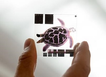
Image Caption: Daniel Corzo has developed an inkjet-printing approach to fabricate high-efficiency organic solar cells at a large scale.
Organic photovoltaic materials could soon replace inorganic semiconductors in solar-powered devices because of their lightness, flexibility and low cost. These materials are easy to modify and process in solution, which makes them highly attractive for customization and large-scale production. In particular, customized solar cell designs can be used in conjunction with other printed electronics to power a plethora of applications, such as disposable electronics, intelligent packaging, interactive printed media and lab-on-a-chip devices.
Nonfullerene acceptors are emerging materials that have helped boost the efficiency of organic solar cells close to commercialization. These components are typically blended with electron donors in a light-responsive electrochemical layer. They have proven effective for drawing the light-generated pairs of electrons and negatively charged holes apart and maintaining electric current when exposed to sunlight. However, scale-up and manufacturing challenges have hindered efforts to transfer these materials from the laboratory to industrial and consumer-ready scales.
To bridge this gap, Derya Baran and her colleagues have engineered inkjet-printable solar materials containing a nonfullerene acceptor and deposited these inks over large areas to produce photovoltaic cells. The resulting devices achieved efficiencies of six percent, which is comparable to the efficiencies of their spin-coated analogs.
Ph.D. candidate Daniel Corzo explains that inkjet printing presents several advantages over traditional spin-coating and blade-coating deposition techniques, including low material consumption and rapid design changes through digital platforms. “This enables low-cost manufacturing, patterning into complex shapes, and multilayered device fabrication without the need for multistep lithography,” he adds.
The researchers optimized the printing process by tuning the viscosity and evaporation behavior of the ink to improve both how the droplets were ejected and how they interacted with the substrate surface. According to Corzo, this optimization has provided a repeatable and commercially scalable process.
This bale of turtles is in fact a collection of inkjet-printed solar cells that show a conversion efficiency of 4.76%.
Baran’s team also fabricated high-efficiency turtle-shaped devices, demonstrating the potential for the process to be customized. “It is amazing that we can now fabricate solar cells with complex shapes at the push of a button, opening the door to a wide variety of applications,” Corzo says.
The researchers are currently developing fully printed organic solar cells and enhancing cell efficiency using higher-performance materials. They are also investigating ways to integrate the devices in modules and with other printed electronics for self-powered autonomous sensing.
Share on:


Subscribe
Stay ahead of the technologies shaping the future of electronics with our latest newsletter, Advanced Electronics Packaging Digest. Get expert insights on advanced packaging, materials, and system-level innovation, delivered straight to your inbox.
Subscribe now to stay informed, competitive, and connected.
Suggested Items
AI Demand Drives PCB Material Market Growth
05/08/2026 | TPCAAs AI computing continues to drive a comprehensive upgrade in hardware specifications, the global printed circuit board industry is undergoing a profound structural transformation.
I-Connect007 Editor’s Choice: Five Must-Reads for the Week
05/01/2026 | Michelle Te, I-Connect007If it feels like the PCB industry is accelerating faster than ever, you’re not imagining it. From advanced materials driven by AI applications to renewed investment in domestic manufacturing—and the next generation stepping into critical roles—there’s a lot shifting at once. My selections for this week highlight where the pressure points are forming, and where the opportunities are emerging.
Electronics Manufacturing Needs Your Voice: Global Sentiment Survey Now Live
04/30/2026 | Global Electronics AssociationThe latest monthly Global Sentiment Survey from the Global Electronics Association is now open. At a time when demand uncertainty, policy shifts, energy costs, and supply chain recalibration are pulling the industry in multiple directions, the survey captures something macroeconomic data often misses: how manufacturers are actually experiencing conditions on the ground.
From Backbone to Breakthroughs: I-Connect007 Wraps PCB Materials Series with Focus on Innovation
05/06/2026 | I-Connect007I-Connect007 wraps up its six-part podcast series, PCB Materials: The Backbone and Future of Electronics, with Episode 6 and a discussion focusing on innovation. In Episode 6, Marcy LaRont speaks with Isola CTO Kirk Thompson about a critical turning point for the PCB industry as innovation accelerates. As data rates climb and demands from AI infrastructure, power density, flexible electronics, photonics, and chiplet integration intensify, traditional material assumptions are no longer sufficient.
Jiva Soluboard Getting the Attention It Deserves
04/30/2026 | Marcy LaRont, I-Connect007 MagazineJiva is a newer company that bridges the divide between PCB fabrication and product circularity or sustainability. Jiva Soluboard is the first fully recyclable laminate material ever created for PCB fabrication, and it's not going unnoticed. Stephen Driver, CEO of Jiva, gave us an update at APEX EXPO, including an exciting certification achievement in February.