


 Dan’s Biz Bookshelf: ‘Abundance: How We Build a Better Future’
 Trouble in Your Tank: In Complex Systems, Design Rules Aren’t Optional
 It’s Only Common Sense: The Phone Is Still Your Competitive Advantage


Tune in to Future Polarity Quantum Devices
June 13, 2019 | ICN2Estimated reading time: 2 minutes
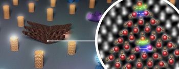
A thorough study published in NanoLetters and led by the ICN2 Advanced Electron Nanoscopy group provides new insights on the growth mechanisms and conditions that determine the polarity of semiconductor nanostructures. Fine control of polarity can result in the design of new quantum devices.
Future applications of nanomaterials depend on our ability to understand their characteristics at the atomic scale and to modulate them at will. Polarity appears to play an important role in determining the physical and morphological properties of semiconductor nanostructures, thus researchers are studying how to control or change it.
Because of the way atoms are arranged in crystal structures, electromagnetic charges are locally separated. As a consequence, if we look at the crystal along specific directions, we can observe oppositely-charged ionic couples, which are called dumbbells because of their shape. Binary compounds—i.e. formed by two elements only—are said to have A- or B- polarity according to the dumbbell orientation. The type of polarity of these materials influences their properties, which, in turn, have a remarkable impact on the final applications.
An extensive study on polarity of semiconductor materials, conducted by Dr. María de la Mata, ICREA Prof. Jordi Arbiol and Sara Martí-Sánchez from the ICN2 Advanced Electron Nanoscopy group, in collaboration with researchers at the École Polytechnique Fédérale of Lausanne (Switzerland), the University of Bremen (Germany), the Nanyang Technological University (Singapore) and the Microsoft Quantum Lab of Delft (The Netherlands), has been recently published on NanoLetters.
Nanostructures of a wide range of semiconductor compounds have been grown in laboratory and then analyzed, using scanning transmission electron microscopy, in order to determine their polarity and compile a complete mapping. The researchers have observed that most of these materials spontaneously grow along the B-polar direction, while only a few follow either A- or B- polar directions. The latter are particularly interesting, as potentially they could offer us the possibility to predetermine their polarity during growth by intervening on some variables.
The aim of this study was indeed to pin down the factors that influence the polarity of non-planar nanostructures. Since, from the analysis of the new results and previously reported data, did not emerge any parameter that would relate the type of polarity with a specific family of binary compounds, it was concluded that the observed polarity of these nanostructures is strictly connected to the growth conditions and techniques.
Experiments have been carried out using both particle-assisted and non-particle-assisted growth techniques, which differ in the structure development starting from a core of solid material or not, and varying other parameters. Even though a complete comprehension of the dynamic and kinetics of the growing process has not been achieved yet, this study moves forward our knowledge of the mechanisms determining the growth polarity at the nanoscale. It also provides an overview of the parameters that can be tuned during the growth to influence the polarity of the resulting nanostructure. Once a fine control capability is reached, it will be possible to engineer new structures with preselected or changeable polarity with the aim to develop novel quantum devices.
Share on:


Subscribe
Stay ahead of the technologies shaping the future of electronics with our latest newsletter, Advanced Electronics Packaging Digest. Get expert insights on advanced packaging, materials, and system-level innovation, delivered straight to your inbox.
Subscribe now to stay informed, competitive, and connected.
Suggested Items
AI Demand Drives PCB Material Market Growth
05/08/2026 | TPCAAs AI computing continues to drive a comprehensive upgrade in hardware specifications, the global printed circuit board industry is undergoing a profound structural transformation.
I-Connect007 Editor’s Choice: Five Must-Reads for the Week
05/01/2026 | Michelle Te, I-Connect007If it feels like the PCB industry is accelerating faster than ever, you’re not imagining it. From advanced materials driven by AI applications to renewed investment in domestic manufacturing—and the next generation stepping into critical roles—there’s a lot shifting at once. My selections for this week highlight where the pressure points are forming, and where the opportunities are emerging.
Electronics Manufacturing Needs Your Voice: Global Sentiment Survey Now Live
04/30/2026 | Global Electronics AssociationThe latest monthly Global Sentiment Survey from the Global Electronics Association is now open. At a time when demand uncertainty, policy shifts, energy costs, and supply chain recalibration are pulling the industry in multiple directions, the survey captures something macroeconomic data often misses: how manufacturers are actually experiencing conditions on the ground.
From Backbone to Breakthroughs: I-Connect007 Wraps PCB Materials Series with Focus on Innovation
05/06/2026 | I-Connect007I-Connect007 wraps up its six-part podcast series, PCB Materials: The Backbone and Future of Electronics, with Episode 6 and a discussion focusing on innovation. In Episode 6, Marcy LaRont speaks with Isola CTO Kirk Thompson about a critical turning point for the PCB industry as innovation accelerates. As data rates climb and demands from AI infrastructure, power density, flexible electronics, photonics, and chiplet integration intensify, traditional material assumptions are no longer sufficient.
Jiva Soluboard Getting the Attention It Deserves
04/30/2026 | Marcy LaRont, I-Connect007 MagazineJiva is a newer company that bridges the divide between PCB fabrication and product circularity or sustainability. Jiva Soluboard is the first fully recyclable laminate material ever created for PCB fabrication, and it's not going unnoticed. Stephen Driver, CEO of Jiva, gave us an update at APEX EXPO, including an exciting certification achievement in February.