


 It’s Only Common Sense: Marketing Isn’t Fluff, It’s Ammunition
 Driving Innovation: Mechanical and Optical Processes During Rigid-flex Production
 The Chemical Connection: Onshoring PCB Production—Daunting but Certainly Possible


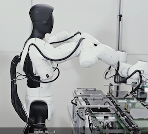
Building the Tools of the Next Manufacturing Revolution
June 18, 2019 | MITEstimated reading time: 6 minutes
To be sure, “It’s not that 3-D printing will replace all of manufacturing or even a tenth of it in the near future,” Hart says. “It is the cornerstone of a digital transformation in the way we go about designing, producing, and servicing products in a responsive, market-driven manner.”
As these new technologies become more widely used, the resulting changes in industrial manufacturing processes could have profound implications for the workers of the future, and for their training and education. Hart is deeply engaged with those questions, too.
“We also like to think at the system level, in terms of economic modeling of new manufacturing technologies including 3-D printing, and understanding how companies work and what transformations may be needed in product-development processes and in the skills of their employees,” he says.
That research has been inspired by Hart’s involvement in MIT’s Work of the Future initiative, for which he’s assembled a team to examine how demands on workers across the product life cycle — from the designer to the engineer to the production worker — will be influenced by the rise of automation and digitization.
Hart’s own workflow has become ever more diverse, in pace with the rapid developments in the field. But his teaching, research, and work with industry all go hand in hand, he says. “It’s all symbiotic. All these activities and interests feed to and from one another. We also have a prime responsibility to consider the sustainability of the manufacturing technologies that we develop, and the implications of more flexible manufacturing — both positive and negative — on the resource pressures of the planet.”
In addition to his own experience as an entrepreneur — and becoming co-inventor of more than 50 pending and issued patents — Hart gains insights and energy from teaching industry professionals and students alike.
He’s a recipient of the prestigious Ruth and Joel Spira Award for Distinguished Teaching at MIT, as well as the MIT Keenan Award for Innovation in Undergraduate Education, for his work teaching MIT’s flagship undergraduate manufacturing course 2.008 (Design and Manufacturing) and its equivalent as an open online course on edX. As the Department of Mechanical Engineering’s “Maker Czar,” he oversees the design and manufacturing shops used by hundreds of students, working with instructors and various department leaders to make sure facilities have state-of-the-art equipment and capabilities and that students become proficient with both established and emerging technologies.
He also created and leads an online MITxPro course for professionals, “Additive Manufacturing for Innovative Design and Production,” which has enrolled over 2,500 participants from around the world who have sought to learn the fundamentals and applications of 3-D printing and apply this knowledge to their jobs.
“The experience of teaching and developing courses for industry, both in person and digitally, has been incredibly helpful in shaping my perspective of how we at MIT can contribute to the future of manufacturing,” Hart says.
Page 2 of 2Share on:


Testimonial
"Your magazines are a great platform for people to exchange knowledge. Thank you for the work that you do."
Simon Khesin - Schmoll MaschinenSuggested Items
WestDev Announces Advanced Thermal Analysis Integration for Pulsonix PCB Design Suite
10/29/2025 | WestDev Ltd.Pulsonix, the industry-leading PCB design software from WestDev Ltd., announced a major enhancement to its design ecosystem: a direct interface between Pulsonix and ADAM Research's TRM (Thermal Risk Management) analysis software.
Designers Notebook: Power and Ground Distribution Basics
10/29/2025 | Vern Solberg -- Column: Designer's NotebookThe principal objectives to be established during the planning stage are to define the interrelationship between all component elements and confirm that there is sufficient surface area for placement, the space needed to ensure efficient circuit interconnect, and to accommodate adequate power and ground distribution.
Episode 6 of Ultra HDI Podcast Series Explores Copper-filled Microvias in Advanced PCB Design and Fabrication
10/15/2025 | I-Connect007I-Connect007 has released Episode 6 of its acclaimed On the Line with... American Standard Circuits: Ultra High Density Interconnect (UHDI) podcast series. In this episode, “Copper Filling of Vias,” host Nolan Johnson once again welcomes John Johnson, Director of Quality and Advanced Technology at American Standard Circuits, for a deep dive into the pros and cons of copper plating microvias—from both the fabricator’s and designer’s perspectives.
Nolan’s Notes: Tariffs, Technologies, and Optimization
10/01/2025 | Nolan Johnson -- Column: Nolan's NotesLast month, SMT007 Magazine spotlighted India, and boy, did we pick a good time to do so. Tariff and trade news involving India was breaking like a storm surge. The U.S. tariffs shifted India from one of the most favorable trade agreements to the least favorable. Electronics continue to be exempt for the time being, but lest you think that we’re free and clear because we manufacture electronics, steel and aluminum are specifically called out at the 50% tariff levels.
MacDermid Alpha & Graphic PLC Lead UK’s First Horizontal Electroless Copper Installation
09/30/2025 | MacDermid Alpha & Graphic PLCMacDermid Alpha Electronics Solutions, a leading supplier of integrated materials and chemistries to the electronics industry, is proud to support Graphic PLC, a Somacis company, with the installation of the first horizontal electroless copper metallization process in the UK.