


 Dan’s Biz Bookshelf: ‘Abundance: How We Build a Better Future’
 Trouble in Your Tank: In Complex Systems, Design Rules Aren’t Optional
 It’s Only Common Sense: The Phone Is Still Your Competitive Advantage


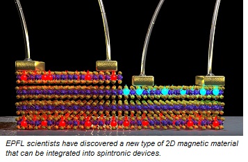
A New 2D Magnet Draws Future Devices Closer
June 19, 2019 | EPFLEstimated reading time: 2 minutes
We are all familiar with the image of electrons zipping around an atom’s nucleus and forming chemical bonds in molecules and materials. But what is less known is that electrons have an additional unique property: spin. It is difficult to make an analogy, but one could crudely describe electron spin as a spinning-top rotating around its axis. But what is even more interesting is that, when spins of electrons align together in a material, this leads to the well-known phenomenon of magnetism.
One of the most cutting-edge fields in technology is spintronics, a still-experimental effort to design and build devices—such as computers and memories—that run on electron spin rather than just the movement of charges (which we know as electrical current). But such applications demand new magnetic materials with new properties. For example, it would be a huge advantage if magnetism occurs in an extremely thin layer of the material—the so-called two-dimensional (2D) materials that include graphene, which is basically an atom-thick layer of graphite.
However, finding 2D magnetic materials is challenging. Chromium iodide (CrI3) recently revealed many interesting properties, but it degrades rapidly in ambient conditions and its insulating nature doesn’t promise much in the way of spintronics applications, most of which require metallic and air-stable magnetic materials.
Now, the groups of Andras Kis and Oleg Yazyev at EPFL have found a new metallic and air-stable 2D magnet: platinum diselenide (PtSe2). The discovery was made by Ahmet Avsar, a postdoc in Kis’s lab, who was actually looking into something else entirely.
To explain the discovery of magnetism in PtSe2, the researchers first used calculations based on density functional theory, a method that models and studies the structure of complex systems with many electrons, such as materials and nanostructures. The theoretical analysis showed that the magnetism of PtSe2 is caused by the so-called “defects” on its surface, which are irregularities in the arrangement of atoms. “More than a decade ago, we found a somewhat similar scenario for defects in graphene, but PtSe2 was a total surprise for us,” says Oleg Yazyev.
The researchers confirmed the presence of magnetism in the material with a powerful magneto-resistance measurement technique. The magnetism was surprising, since perfectly crystalline PtSe2 is supposed to be non-magnetic. “This is the first time that defect-induced magnetism in this type of 2D materials is observed,” says Andras Kis. “It expands the range of 2D ferromagnets into materials that would otherwise be overlooked by massive database-mining techniques.”
Removing or adding one layer of PtSe2 is enough to change the way spins talk to each other across layers. And what makes it even more promising, is the fact that its magnetism, even within the same layer, can be further manipulated by strategically placing defects across its surface—a process known as “defect engineering” that can be accomplished by irradiating the material’s surface with electron or proton beams.
“Such ultra-thin metallic magnets could be integrated into the next generation spin-transfer torque magnetic random-access memory [STT MRAM] devices”, says Ahmet Avsar. “2D magnets could reduce the critical current required to change magnetic polarity, and help us with further miniaturization. These are the major challenges that companies are hoping to solve.”
Share on:


Subscribe
Stay ahead of the technologies shaping the future of electronics with our latest newsletter, Advanced Electronics Packaging Digest. Get expert insights on advanced packaging, materials, and system-level innovation, delivered straight to your inbox.
Subscribe now to stay informed, competitive, and connected.
Suggested Items
AI Demand Drives PCB Material Market Growth
05/08/2026 | TPCAAs AI computing continues to drive a comprehensive upgrade in hardware specifications, the global printed circuit board industry is undergoing a profound structural transformation.
I-Connect007 Editor’s Choice: Five Must-Reads for the Week
05/01/2026 | Michelle Te, I-Connect007If it feels like the PCB industry is accelerating faster than ever, you’re not imagining it. From advanced materials driven by AI applications to renewed investment in domestic manufacturing—and the next generation stepping into critical roles—there’s a lot shifting at once. My selections for this week highlight where the pressure points are forming, and where the opportunities are emerging.
Electronics Manufacturing Needs Your Voice: Global Sentiment Survey Now Live
04/30/2026 | Global Electronics AssociationThe latest monthly Global Sentiment Survey from the Global Electronics Association is now open. At a time when demand uncertainty, policy shifts, energy costs, and supply chain recalibration are pulling the industry in multiple directions, the survey captures something macroeconomic data often misses: how manufacturers are actually experiencing conditions on the ground.
From Backbone to Breakthroughs: I-Connect007 Wraps PCB Materials Series with Focus on Innovation
05/06/2026 | I-Connect007I-Connect007 wraps up its six-part podcast series, PCB Materials: The Backbone and Future of Electronics, with Episode 6 and a discussion focusing on innovation. In Episode 6, Marcy LaRont speaks with Isola CTO Kirk Thompson about a critical turning point for the PCB industry as innovation accelerates. As data rates climb and demands from AI infrastructure, power density, flexible electronics, photonics, and chiplet integration intensify, traditional material assumptions are no longer sufficient.
Jiva Soluboard Getting the Attention It Deserves
04/30/2026 | Marcy LaRont, I-Connect007 MagazineJiva is a newer company that bridges the divide between PCB fabrication and product circularity or sustainability. Jiva Soluboard is the first fully recyclable laminate material ever created for PCB fabrication, and it's not going unnoticed. Stephen Driver, CEO of Jiva, gave us an update at APEX EXPO, including an exciting certification achievement in February.