


 Dan’s Biz Bookshelf: ‘Abundance: How We Build a Better Future’
 Trouble in Your Tank: In Complex Systems, Design Rules Aren’t Optional
 It’s Only Common Sense: The Phone Is Still Your Competitive Advantage


Photovoltaic Nanotubes
June 20, 2019 | University of TokyoEstimated reading time: 3 minutes
Physicists discovered a novel kind of nanotube that generates current in the presence of light. Devices such as optical sensors and infrared imaging chips are likely applications, which could be useful in fields such as automated transport and astronomy. In future, if the effect can be magnified and the technology scaled up, it could lead to high-efficiency solar power devices.
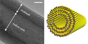
Image Caption: Transmission electron microscopy image of a hollow core nanotube. The white scale bar corresponds to 10 nanometers (left). Rendering of a nanotube (right).
Working with an international team of physicists, University of Tokyo Professor Yoshihiro Iwasa was exploring possible functions of a special semiconductor nanotube when he had a lightbulb moment. He took this proverbial lightbulb (which was in reality a laser) and shone it on the nanotube to discover something enlightening. Certain wavelengths and intensities of light induced a current in the sample — this is called the photovoltaic effect. There are several photovoltaic materials, but the nature and behavior of this nanotube is cause for excitement.
“Essentially our research material generates electricity like solar panels, but in a different way,” said Iwasa. “Together with Dr. Yijin Zhang from the Max Planck Institute for Solid State Research in Germany, we demonstrated for the first time nanomaterials could overcome an obstacle that will soon limit current solar technology. For now solar panels are as good as they can be, but our technology could improve upon that.”
The current-inducing nanotube is made from rolled-up sheets of a special semiconductor material based on tungsten disulfide (WS2). The sheets do not induce a current in the presence of light unless rolled into tubes. This is an emergent behavior, one not intrinsic to the material until it’s modified. What is interesting is how it differs from existing photovoltaic materials.
Generally, photovoltaic solar panels make use of a certain arrangement of materials called a p-n junction. This is where two different kinds of materials (p-type and n-type) are attached, which alone do not generate a current in the presence of light, but when placed together, do. P-n junction-based photovoltaics have improved in efficiency over the 80 years or so since their discovery. However, they are getting close to their theoretical limits due in part to their need for the arrangement of multiple materials.
WS2 nanotubes do not rely on a junction between materials to gain the photovoltaic effect. When exposed to light, they generate a current throughout their entire structure or bulk. This is called the bulk photovoltaic effect (BPVE) and it occurs as the WS2 nanotube is not symmetrical if you were to reverse it. If it were symmetrical, the current induced would not have a preferred direction and thus would not flow. So other symmetrical nanotubes — such as the famous carbon nanotubes — don't exhibit BPVE despite being great electrical conductors.
Four inset images. The lower right is a coarse grey texture. The other othree are orange geometric shapes on dark backgrounds.
Image Caption: Various iterations of the experimental nanotube device. Images captured by an atomic force microscope, and a scanning Kelvin probe microscope (lower right).
“Our research shows an entire order of magnitude improvement in efficiency of BPVE compared to its presence in other materials,” continued Iwasa. “But despite this huge gain, our WS2 nanotube cannot yet compare to the generating potential of p-n junction materials. This is because the device is nanoscopic and will be difficult to make larger. But it is possible and I hope chemists are inspired to take on that challenge.”
In the long term, researchers hope this kind of material could allow fabrication of more efficient solar panels. But given the foreseeable size constraints in the near term, it’s more likely to find use in other applications. BVPE could be used to create more sensitive and higher-fidelity optical or infrared sensors. These have further applications in embedded monitoring devices, sensor-laden self-driving cars or even in the imaging sensors for astronomical telescopes.
“My colleagues from around the world and I eagerly explore the potential of this unprecedented technology,” concluded Iwasa. “For me, the idea of creating new materials beyond anything nature could provide is a fascinating reward in its own right.”
Share on:


Subscribe
Stay ahead of the technologies shaping the future of electronics with our latest newsletter, Advanced Electronics Packaging Digest. Get expert insights on advanced packaging, materials, and system-level innovation, delivered straight to your inbox.
Subscribe now to stay informed, competitive, and connected.
Suggested Items
Sony Semiconductor Solutions, TSMC Enter Preliminary Agreement for Next-Generation Image Sensor Strategic Partnership
05/08/2026 | TSMCSony Semiconductor Solutions Corporation and TSMC announced the signing of a non-binding memorandum of understanding (MOU) to form a strategic partnership for the development and manufacturing of next-generation image sensors.
BGA Technology Expands Inspection Capabilities with Creative Electron TruView X-ray System
05/08/2026 | BGA TechnologyBGA Technology, a leading provider of advanced electronics testing and inspection services, has enhanced its inspection capabilities with the addition of a Creative Electron TruView™ Simplex X-ray system at its Holbrook, New York facility.
Molex Completes Acquisition of Teramount Ltd.
05/07/2026 | PRNewswireMolex, a global electronics leader and connectivity innovator, has completed the acquisition of Teramount Ltd., an Israel‑based developer of detachable fiber‑to‑chip connectivity solutions optimized for high‑volume Co‑Packaged Optics (CPO) and other silicon photonics applications.
IBM, Aramco Explore Collaboration to Accelerate AI and Innovation Across Saudi Arabia
05/07/2026 | IBMAramco and IBM announced their intended collaboration on opportunities to advance artificial intelligence, agentic AI, automation, material science and other mutually agreed domains in the industrial sector.
Foxconn Launches Second-Gen LEO Satellite, Begins Inter-Satellite Link Testing
05/05/2026 | FoxconnFoxconn Technology Group, the world's largest electronics manufacturing services provider, announced that its second-generation low-Earth orbit (LEO) satellites, "Pearl-1A" and "Pearl-1B," were successfully launched into their designated orbits via SpaceX's Falcon 9 rocket on the evening of May 3 (Taipei time).