


 Dan’s Biz Bookshelf: ‘Abundance: How We Build a Better Future’
 Trouble in Your Tank: In Complex Systems, Design Rules Aren’t Optional
 It’s Only Common Sense: The Phone Is Still Your Competitive Advantage


Hidden Chargers
June 20, 2019 | University of TokyoEstimated reading time: 2 minutes
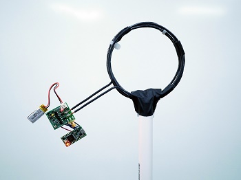
Researchers from the University of Tokyo led by doctoral student Takuya Sasatani, Disney Research and the University of Michigan in the U.S., created and demonstrated a room-sized device which uses magnetic fields to charge compatible devices inside it.
“The internet of things is coming,” says Sasatani. “People will soon find their environments populated by small sensors and other devices which need power and communication. We have a safe and elegant solution for this, and it too could help technology become more invisible.”
The roomwide wireless power transfer system can simultaneously charge multiple devices—or nodes—within the confines of a room. Metal sheets and electrical components are embedded within a column in the center of the room and the structure of the room itself. As the functional elements of the system are integrated into a room, this approach is most suited for inclusion in new buildings, although the research team also explore ways to retrofit existing environments.
For the system to work, researchers exploit a phenomenon called quasistatic cavity resonance. Here, oscillating magnetic fields confined to a certain volume induce the flow of charge in devices possessing specially designed coils. The magnetic field swirls around the room and the electric field is confined to the components embedded within the central pole.
“Safety is our prime concern and we will make sure that future deployments of our system meet all governmental regulations for health and safety. We use magnetic fields well within safety limits for human proximity and the electric field is isolated by capacitors in the central column,” continues Sasatani. “Conversely, the presence of people should not affect power transfer efficiency. It even plays well with Wi-Fi, though our system provides an alternative communication link with small power consumption. This can drastically extend battery life of the numerous low-power devices installed in our surroundings.”
An essential feature of devices such as sensors is they communicate their data periodically. The researchers engineered a way for compatible devices to send and receive data through the same mechanism which powers them. Compatible devices communicate with the central system at several kilobits per second by modulating a power signal in a method analogous to how AM radio works. While not yet suitable to stream videos, it’s enough to communicate many kinds of ambient data that sensors are likely to collect.
“The combined power and data capacity of our system potentially makes it suitable for environments such as hospitals, greenhouses, labs, event spaces or your home,” concludes Sasatani. “We will continue to innovate and improve power transfer loads and communication bandwidth, while ensuring compatible devices will be cheap and easy to manufacture.”
As well as being cheap to manufacture, the system should also prove inexpensive to run, using about 10 watts of power, equivalent to an efficient LED lightbulb.
Share on:


Subscribe
Stay ahead of the technologies shaping the future of electronics with our latest newsletter, Advanced Electronics Packaging Digest. Get expert insights on advanced packaging, materials, and system-level innovation, delivered straight to your inbox.
Subscribe now to stay informed, competitive, and connected.
Suggested Items
Northrop Grumman Advances Improved Threat Detection System for US Army
05/07/2026 | Northrop GrummanNorthrop Grumman Corporation was awarded a U.S. Army contract for second phase development of its Improved Threat Detection System (ITDS).
Renesas Completes Acquisition of Irida Labs
05/07/2026 | RenesasRenesas Electronics Corporation, a premier supplier of advanced semiconductor solutions, announced that a subsidiary of Renesas has completed the acquisition of Irida Labs, a Greece-based company specializing in embedded software for AI-powered visual perception systems.
More Than Electrical Test: TTCI to Spotlight X-ray and CT Capabilities at SMTA Capital Expo
05/07/2026 | TTCIThe Training Connection LLC (TTC-LLC) will exhibit at the SMTA Capital Expo on Thursday, May 14 at the DoubleTree by Hilton Baltimore - BWI Airport.
Green Circuits Heads to Peterson SFB to Support Next-Gen Space and Defense Electronics
05/05/2026 | Green CircuitsThe event, hosted at Peterson Space Force Base, brings together key personnel and mission partners supporting critical U.S. defense and space operations.
ANELLO Photonics Raises $25M to Scale GPS-Denied Navigation Solutions
05/04/2026 | PRNewswireANELLO Photonics, the creator of the Silicon Photonics Optical Gyroscope (SiPhOG) and a leader in solid-state, high-precision inertial navigation systems, today announced it has secured an additional $25 million in a Series B-2 financing round.