


 Dan’s Biz Bookshelf: ‘Abundance: How We Build a Better Future’
 Trouble in Your Tank: In Complex Systems, Design Rules Aren’t Optional
 It’s Only Common Sense: The Phone Is Still Your Competitive Advantage


Novel Via-Hole-Less Multilevel Metal Interconnection Methods
June 24, 2019 | KAISTEstimated reading time: 2 minutes
Forming reliable multi-level metal interconnections is a key technology for integrating devices into organic integrated circuits (ICs). The conventional approach, called “via-hole,” locally removes the insulator and utilizes metal interconnects through the holes.
Due to the high sensitivity of organic materials to chemical solvents, heat, and photo-radiation used in conventional “via-hole” methods, alternative printing methods or laser drilling methods have been developed. However, finding a reliable and practical metal interconnection for organic ICs is still challenging.
The research team of KAIST Professor Sung Gap Im and Postech Professor Kim Jae-Joon reported a new interconnection method that does not require via-hole formation, “via-hole-less metal interconnection,” in Nature Communications on June 3.
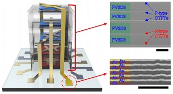
Metal electrodes in different layers can be isolated from each other by patterned dielectric layers, where they then can be interconnected to others in the open area where the dielectric layer is not present. See the images below. Vapor phase deposition and in-situ patterning of dielectric layer using iCVD (initiated chemical vapor deposition), used in the “via-hole-less” method, ensure a damage-free process for organic semiconductor materials and result in outstanding performance of the organic devices as multilevel metal interconnects are reliably formed. The team successfully demonstrated three-dimensional (3D) stacking of five organic transistors and integrated circuits using the proposed via-hole-less interconnect method. See the image below.
Vapor phase deposition and in-situ patterning of dielectric layer using iCVD (initiated chemical vapor deposition), used in the “via-hole-less” method, ensure a damage-free process for organic semiconductor materials and result in outstanding performance of the organic devices as multilevel metal interconnects are reliably formed. The team successfully demonstrated three-dimensional (3D) stacking of five organic transistors and integrated circuits using the proposed via-hole-less interconnect method.
Professor Kim explained, “Our proposed via-hole-less interconnect method using a selectively patterned dielectric overcomes the limitations of the previous time-consuming, one-by-one via-hole formation process and provides reliable methods for creating metal interconnects in organic ICs. We expect the via-hole-less scheme to bring advances to organic IC technology.”
Share on:


Subscribe
Stay ahead of the technologies shaping the future of electronics with our latest newsletter, Advanced Electronics Packaging Digest. Get expert insights on advanced packaging, materials, and system-level innovation, delivered straight to your inbox.
Subscribe now to stay informed, competitive, and connected.
Suggested Items
Market Insights with Pluritec's Maurizio Bonati
04/23/2026 | Real Time with... APEX EXPONolan Johnson interviews Maurizio Bonati, VP of Sales at Pluritec, at APEX EXPO 2026. Bonati details Pluritec's three product divisions, covering a broad spectrum of PCB manufacturing. He discusses the current robust electronics market, driven by AI applications in Asia and technological investments in North America, while noting slower demand in Europe. The interview highlights key sectors like data centers, AI, and medical that benefit from advanced electronics.
AI, HDI, and Interconnect Optimization with MKS' ESI
04/23/2026 | Real Time with... APEX EXPOThis discussion revolves around the transformative impact of AI on HDI and substrate manufacturing. Casey Krueger explains the company's "Optimize the Interconnect" initiative, which features Atotech, to provide a comprehensive solution from pretreatment to laser drilling. MKS' ESI offers the innovative Geode G2 platform which is an advanced laser drilling technology that enhances productivity, reduces energy consumption, and addresses complex design challenges in processing both PCB and ICP materials.
Driving Innovation: Size Matters—Navigating the Challenges of XXL PCB Production
03/02/2026 | Kurt Palmer -- Column: Driving InnovationIn high-end electronics, complexity is often measured in microns. However, when those microns are spread across a massive surface area, the engineering challenge fundamentally changes. Imagine two panels: Both are highly complex, featuring 4-stage build-ups, 2-mil line and space patterns, 2-mil microvias, and through-holes with a demanding 1:30 aspect ratio.
Zhen Ding Holding and Topoint Technology Sign Strategic Cooperation Agreement
12/02/2025 | Zhen Ding TechnologyZhen Ding Tech. Group, the world’s largest PCB manufacturer, and Topoint Technology Co., Ltd., a global leader in precision drill bits and integrated drilling solutions, officially signed a strategic cooperation agreement at the Zen Ding Times Building in Shenzhen.
Simon Khesin: A PCB Journey of Familiar and Unfamiliar Paths
11/24/2025 | Marcy LaRont, PCB007 MagazineIn Driving Innovation, Simon Khesin shares his extraordinary path from Moscow engineer to global account manager at Schmoll Maschinen. His story spans risk, reinvention, and resilience—from designing drilling machines to starting over in Germany—and celebrates the freedom to create and the power of staying adaptable in a changing world.