


 Dan’s Biz Bookshelf: ‘Abundance: How We Build a Better Future’
 Trouble in Your Tank: In Complex Systems, Design Rules Aren’t Optional
 It’s Only Common Sense: The Phone Is Still Your Competitive Advantage


Researchers Explain Visible Light from 2D Lead Halide Perovskites
June 26, 2019 | University of HoustonEstimated reading time: 2 minutes
Researchers drew attention three years ago when they reported that a two-dimensional perovskite—a material with a specific crystal structure—composed of cesium, lead and bromine emitted a strong green light.
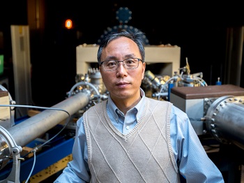
Image Caption: Jiming Bao, associate professor of electrical and computer engineering, led an international group of researchers investigating how a two-dimensional perovskite composed of cesium, lead and bromine was able to emit a strong green light.
Crystals that produce light on the green spectrum are desirable because green light, while valuable in itself, can also be relatively easily converted to other forms that emit blue or red light, making it especially important for optical applications ranging from light-emitting devices to sensitive diagnostic tools.
But there was no agreement about how the crystal, CsPB2Br5, produced the green photoluminescence. Several theories emerged, without a definitive answer.
Now, however, researchers from the United States, Mexico and China, led by an electrical engineer from the University of Houston, have reported in the journal Advanced Materials they have used sophisticated optical and high-pressure diamond anvil cell techniques to determine not only the mechanism for the light emission but also how to replicate it.
They initially synthesized CsPB2Br5 from a related material known as CsPbBr3 and found that the root cause of the light emission is a small overgrowth of nanocrystals composed of that original material, growing along the edge of the CsPB2Br5 crystals. While CsPbBr3, the base crystal, is three-dimensional and appears green under ultraviolet light, the new material, CsPB2Br5, has a layered structure and is optically inactive.
“Now that the mechanism for emitting this light is understood, it can be replicated,” said Jiming Bao, associate professor of electrical and computer engineering at UH and corresponding author on the paper. “Both crystals have the same chemical composition, much like diamond versus graphite, but they have very different optical and electronic properties. People will be able to integrate the two materials to make better devices.”
Potential applications range from solar cells to LED lighting and other electronic devices.
Bao began working on the problem in 2016, a project that ultimately involved 19 researchers from UH and institutions in China and Mexico. At the time, there were two schools of scientific thought on the light emission from the cesium crystal: that it emitted green light due to a defect, mainly a lack of bromine, rather than the material itself, or that a variation had unintentionally been introduced, resulting in the emission.
His group started with the synthesis of a clean sample by dropping CsPbBr3 powder in water, resulting in sharper-edged crystals. The sharper edges emitted a stronger green light, Bao said.
The researchers then used an optical microscope to study the individual crystals of the compound, which Bao said allowed them to determine that although the compound is transparent, “something was going on at the edge, resulting in the photoluminescence.”
They relied on Raman spectroscopy—an optical technique that uses information about how light interacts with a material to determine the material’s lattice properties—to identify nanocrystals of the original source material, CsPbBr3, along the edges of the crystal as the source of the light.
Bao said CsPbBr3 is too unstable to use on its own, but the stability of the converted form isn’t hampered by the small amount of the original crystal.
The researchers said the new understanding of the light emission will yield new opportunities to design and fabricate novel optoelectronic devices. The techniques used to understand the cesium-lead-halide compound can also be applied to other optical materials to learn more about how they emit light, Bao said.
Share on:


Subscribe
Stay ahead of the technologies shaping the future of electronics with our latest newsletter, Advanced Electronics Packaging Digest. Get expert insights on advanced packaging, materials, and system-level innovation, delivered straight to your inbox.
Subscribe now to stay informed, competitive, and connected.
Suggested Items
AI Demand Drives PCB Material Market Growth
05/08/2026 | TPCAAs AI computing continues to drive a comprehensive upgrade in hardware specifications, the global printed circuit board industry is undergoing a profound structural transformation.
I-Connect007 Editor’s Choice: Five Must-Reads for the Week
05/01/2026 | Michelle Te, I-Connect007If it feels like the PCB industry is accelerating faster than ever, you’re not imagining it. From advanced materials driven by AI applications to renewed investment in domestic manufacturing—and the next generation stepping into critical roles—there’s a lot shifting at once. My selections for this week highlight where the pressure points are forming, and where the opportunities are emerging.
Electronics Manufacturing Needs Your Voice: Global Sentiment Survey Now Live
04/30/2026 | Global Electronics AssociationThe latest monthly Global Sentiment Survey from the Global Electronics Association is now open. At a time when demand uncertainty, policy shifts, energy costs, and supply chain recalibration are pulling the industry in multiple directions, the survey captures something macroeconomic data often misses: how manufacturers are actually experiencing conditions on the ground.
From Backbone to Breakthroughs: I-Connect007 Wraps PCB Materials Series with Focus on Innovation
05/06/2026 | I-Connect007I-Connect007 wraps up its six-part podcast series, PCB Materials: The Backbone and Future of Electronics, with Episode 6 and a discussion focusing on innovation. In Episode 6, Marcy LaRont speaks with Isola CTO Kirk Thompson about a critical turning point for the PCB industry as innovation accelerates. As data rates climb and demands from AI infrastructure, power density, flexible electronics, photonics, and chiplet integration intensify, traditional material assumptions are no longer sufficient.
Jiva Soluboard Getting the Attention It Deserves
04/30/2026 | Marcy LaRont, I-Connect007 MagazineJiva is a newer company that bridges the divide between PCB fabrication and product circularity or sustainability. Jiva Soluboard is the first fully recyclable laminate material ever created for PCB fabrication, and it's not going unnoticed. Stephen Driver, CEO of Jiva, gave us an update at APEX EXPO, including an exciting certification achievement in February.