


 Dan’s Biz Bookshelf: ‘Abundance: How We Build a Better Future’
 Trouble in Your Tank: In Complex Systems, Design Rules Aren’t Optional
 It’s Only Common Sense: The Phone Is Still Your Competitive Advantage


Shell Increases Versatility of Nanowires
June 27, 2019 | HZDREstimated reading time: 3 minutes
Nanowires promise to make LEDs more colorful and solar cells more efficient, in addition to speeding up computers. That is, provided that the tiny semiconductors convert electric energy into light, and vice versa, at the right wavelengths.
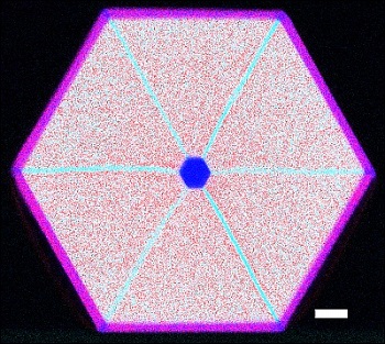
Image Caption: Cross-section of a nanowire featuring a gallium arsenide core, an indium aluminum arsenide shell, and an indium gallium arsenide capping layer (gallium is shaded blue, indium red and aluminum cyan). For comparison, the white bar indicates a scale of 30 nanometers. The image was produced by energy-dispersive X-ray spectroscopy. Source: HZDR/René Hübner;
A research team at Helmholtz-Zentrum Dresden-Rossendorf (HZDR) has managed to produce nanowires with operating wavelengths that can be freely selected over a wide range—simply by altering the shell structure. Fine-tuned nanowires could take on several roles in an optoelectronic component, without having to resort to different materials. That would make the components more powerful, more cost-effective, and easier to integrate, as the team reports in Nature Communications.
Nanowires are extremely versatile. The tiny elements can be used for miniaturized photonic and electronic components in nanotechnology. Applications include optical circuits on chips, novel sensors, LEDs, solar cells and innovative quantum technologies. It is the free-standing nanowires that ensure the compatibility of more recent semiconductor technologies with conventional silicon-based technologies. Since contact to the silicon substrate is tiny, they surmount typical difficulties in combining different materials.
For their study, which lasted several years, the Dresden researchers first set about growing nanowires from the semiconductor material gallium arsenide on silicon substrates. The next step involved enclosing the wafer-thin wires in another layer of material to which they added indium as an additional element. Their goal: the mismatched crystal structure of the materials was intended to induce a mechanical strain in the wire core, which changes the electronic properties of gallium arsenide. For instance, the semiconductor bandgap becomes smaller and the electrons become more mobile. To magnify this effect, the scientists kept adding more indium to the shell, or increased the shell’s thickness. The result went way beyond expectations.
Taking a known effect to extremes
"What we did was take a known effect to extremes,” explained Emmanouil Dimakis, leader of the study that involved researchers from HZDR, TU Dresden and DESY in Hamburg. “The seven percent of strain achieved was tremendous.”
At this level of strain, Dimakis had expected to see disorders occurring in the semiconductors: in their experience, the wire core bends or defects arise. The researchers believe that the special experimental conditions were the reason for the absence of such disorders: First, they grew extremely thin gallium arsenide wires—around five thousand times finer than a human hair. Second, the team managed to produce the wire shell at unusually low temperatures. Surface diffusion of atoms is then more or less frozen, forcing the shell to grow evenly around the core. The team of researchers reinforced their discovery by conducting several independent series of measurements at facilities in Dresden, as well as at the high-brilliance X-ray light sources PETRA III in Hamburg and Diamond in England.
The extraordinary results led the researchers to undertake further investigations: “We shifted our focus to the question of what triggers the extremely high strain in the nanowire core, and how this can be used for certain applications,” Dimakis recollected. “Scientists have been aware of gallium arsenide as a material for years, but nanowires are special. A material may exhibit completely new properties at the nanoscale.”
Potential applications for fiber-optic networks
The researchers realized that the high strain let them shift the bandgap of the gallium arsenide semiconductor to very low energies, making it compatible even for wavelengths of fiber-optic networks. A technological milestone. After all, this spectral range could previously only be achieved via special alloys containing indium, which caused a number of technological problems due to the material mix.
High-precision methods are required to produce nanowires. Four years ago, a special system was installed at HZDR for this purpose: the molecular beam epitaxy laboratory. The self-catalyzed growth of nanowires from beams of atoms or molecules is achieved in the lab; the beams are directed onto silicon substrates in ultra-high-vacuum. Emmanouil Dimakis played a major part in setting up the lab. Most of the studies reported in the current publication were carried out by Leila Balaghi as part of her doctorate.
Share on:


Subscribe
Stay ahead of the technologies shaping the future of electronics with our latest newsletter, Advanced Electronics Packaging Digest. Get expert insights on advanced packaging, materials, and system-level innovation, delivered straight to your inbox.
Subscribe now to stay informed, competitive, and connected.
Suggested Items
Quantum Benchmarking Initiative Expands Quest to Separate Hype from Reality
03/18/2026 | DARPAAs the quantum computing field accelerates, DARPA’s Quantum Benchmarking Initiative (QBI) is expanding to capture its momentum.
Meet the Author Podcast: Martyn Gaudion Unpacks the Secrets of High-Speed PCB Design
07/16/2025 | I-Connect007In this special Meet the Author episode of the On the Line with… podcast, Nolan Johnson sits down with Martyn Gaudion, signal integrity expert, managing director of Polar Instruments, and three-time author in I-Connect007’s popular The Printed Circuit Designer’s Guide to... series.
Intervala Hosts Employee Car and Motorcycle Show, Benefit Nonprofits
08/27/2024 | IntervalaIntervala hosted an employee car and motorcycle show, aptly named the Vala-Cruise and it was a roaring success! Employees had the chance to show off their prized wheels, and it was incredible to see the variety and passion on display.
KIC Honored with IPC Recognition for 25 Years of Membership and Contributions to Electronics Manufacturing Industry
06/24/2024 | KICKIC, a renowned pioneer in thermal process and temperature measurement solutions for electronics manufacturing, is proud to announce that it has been recognized by IPC for 25 years of membership and significant contributions to electronics manufacturing.
Boeing Starliner Spacecraft Completes Successful Crewed Docking with International Space Station
06/07/2024 | BoeingNASA astronauts Barry "Butch" Wilmore and Sunita "Suni" Williams successfully docked Boeing's Starliner spacecraft to the International Space Station (ISS), about 26 hours after launching from Cape Canaveral Space Force Station.