


 Dan’s Biz Bookshelf: ‘Abundance: How We Build a Better Future’
 Trouble in Your Tank: In Complex Systems, Design Rules Aren’t Optional
 It’s Only Common Sense: The Phone Is Still Your Competitive Advantage


Advanced Method for Analyzing Graphene Oxide
July 1, 2019 | Tomsk Polytechnic UniversityEstimated reading time: 2 minutes
Researchers from Tomsk Polytechnic University have developed a reliable method for analyzing the reduction of graphene oxide microregions. In contrast to earlier proposed methods based on Raman spectroscopy, this advanced method provides more exact data about unique properties of certain areas of the material of only a few micrometers in size.
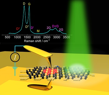
Image Caption: Raman spectrum of graphene oxide with the designation of peaks, and the scheme of the experiment
The international research team led by Professor Raul Rodrigez from TPU School of Chemistry & Applied Biomedical Sciences and Professor Evgeniya Sheremet from TPU School of High Energy Physics is developing new field - optical nanospectroscopy, as well as plasmon and sensor materials development for biomedicine and electronics.
According to Professor Sheremet, the study of unique physical-chemical properties of graphene oxide is still relevant despite many studies in the area. Graphene oxide has a graphene structure with attached oxygen-containing functional groups. The number of these groups strongly influences the properties of the material.
"The fewer oxygen groups remain on the surface of graphene oxide, the higher its reduction. This criterion influences whether the material will be hydrophilic and a dielectric due to polar groups, or it will be more similar to graphene, i.e. hydrophobic and a conductor," says TPU professor.
There are several ways to evaluate the reduction, for example, X-ray photoelectron spectroscopy (XPS) and infrared spectroscopy. However, these methods work only with large areas of materials, whereas microregions are required to process graphene oxide to be applied in electronics. Therefore, TPU scientists investigate laser-reduced graphene oxide, the size of reduced areas can be less than several micrometers.
‘We were looking for a method that allowed us to obtain at least micron resolution, such as Raman spectroscopy,’ explains Evgeniya Sheremet.
Reduced graphene oxide (rGO) was obtained under different laser powers in the range from 0.1 to 10 mW. Then, the researchers investigated reduced areas by using Raman spectrometer and a joint current sensing atomic force microscopy (CSAFM). Raman spectroscopy is widely used for the study of many properties of carbon materials, especially graphene, including mechanical stress, the number of defects, and the type of alloying. However, existing approaches suitable for graphene do not work for graphene oxide since its lattice has a greater number of defects. The analytical methods lose sensitivity in this case.
‘Usually, first-order peaks are analyzed in carbon materials but for graphene oxide, they do not provide reliable results. Therefore, we analyzed the areas of high frequencies and found a clear pattern. The relative intensity of second-order peaks decreases with increasing the extent of reduction. Notably, there is a strong correlation with the conductivity of the material, i.e. we can use Raman signal to assess the reduction of graphene oxide. This is a more reliable method than the earlier proposed ones,’ emphasizes the professor.
Moreover, using nanospectroscopy approaches, this technique can be used for analyzing nanoscale areas.
Share on:


Subscribe
Stay ahead of the technologies shaping the future of electronics with our latest newsletter, Advanced Electronics Packaging Digest. Get expert insights on advanced packaging, materials, and system-level innovation, delivered straight to your inbox.
Subscribe now to stay informed, competitive, and connected.
Suggested Items
AI Demand Drives PCB Material Market Growth
05/08/2026 | TPCAAs AI computing continues to drive a comprehensive upgrade in hardware specifications, the global printed circuit board industry is undergoing a profound structural transformation.
I-Connect007 Editor’s Choice: Five Must-Reads for the Week
05/01/2026 | Michelle Te, I-Connect007If it feels like the PCB industry is accelerating faster than ever, you’re not imagining it. From advanced materials driven by AI applications to renewed investment in domestic manufacturing—and the next generation stepping into critical roles—there’s a lot shifting at once. My selections for this week highlight where the pressure points are forming, and where the opportunities are emerging.
Electronics Manufacturing Needs Your Voice: Global Sentiment Survey Now Live
04/30/2026 | Global Electronics AssociationThe latest monthly Global Sentiment Survey from the Global Electronics Association is now open. At a time when demand uncertainty, policy shifts, energy costs, and supply chain recalibration are pulling the industry in multiple directions, the survey captures something macroeconomic data often misses: how manufacturers are actually experiencing conditions on the ground.
From Backbone to Breakthroughs: I-Connect007 Wraps PCB Materials Series with Focus on Innovation
05/06/2026 | I-Connect007I-Connect007 wraps up its six-part podcast series, PCB Materials: The Backbone and Future of Electronics, with Episode 6 and a discussion focusing on innovation. In Episode 6, Marcy LaRont speaks with Isola CTO Kirk Thompson about a critical turning point for the PCB industry as innovation accelerates. As data rates climb and demands from AI infrastructure, power density, flexible electronics, photonics, and chiplet integration intensify, traditional material assumptions are no longer sufficient.
Jiva Soluboard Getting the Attention It Deserves
04/30/2026 | Marcy LaRont, I-Connect007 MagazineJiva is a newer company that bridges the divide between PCB fabrication and product circularity or sustainability. Jiva Soluboard is the first fully recyclable laminate material ever created for PCB fabrication, and it's not going unnoticed. Stephen Driver, CEO of Jiva, gave us an update at APEX EXPO, including an exciting certification achievement in February.