


 Dan’s Biz Bookshelf: ‘Abundance: How We Build a Better Future’
 Trouble in Your Tank: In Complex Systems, Design Rules Aren’t Optional
 It’s Only Common Sense: The Phone Is Still Your Competitive Advantage


X-Rays Reveal Monolayer Phase in Organic Semiconductor
July 8, 2019 | MIPTEstimated reading time: 3 minutes
A team of researchers from Russia, Germany, and France featuring materials scientists from the Moscow Institute of Science and Technology has investigated how the electrical properties of dihexyl-quaterthiophene thin films depend on their structure.
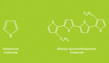
Figure 1. Structural formulas of the thiophene and dihexyl-quarterthiophene molecules. (Image: Elena Khavina/MIPT)
This material is an organic semiconductor with prospects for flexible electronics. It turned out that once the thin films undergo a transition from the crystal to the liquid-crystal state, they lose some of their electrical conductivity.
The team also discovered a “third phase” that does not occur in bulk material and corresponds to a monomolecular layer of the semiconductor. This structure could be favorable for charge transport across the films, with potential implications for microelectronics design.
The research findings were published in Nanoscale Research Letters ("Phase Transitions and Formation of a Monolayer-Type Structure in Thin Oligothiophene Films: Exploration with a Combined In Situ X-ray Diffraction and Electrical Measurements").
Oligothiophenes are promising organic semiconductors. Their rod-shaped molecules can orient at the surface on which they have been deposited, piling up cycles of hydrocarbons containing a sulfur atom known as thiophenes, like stacks of coins. The “coin edges” in the neighboring stacks form a herringbone pattern. This molecular arrangement enables the charge transfer from one molecule to the other.
As the number of thiophenes in the molecule increased, so does the electrical conductivity, at the cost of the compound’s solubility. Four is believed to be the optimal number of these so-called thiophene moieties. To increase solubility, hexyl fragments are grafted to the ends of the conjugated molecular fragment (Fig. 1).
The researchers dissolved and evaporated dihexyl-quarterthiophene (DH4T) in a vacuum reactor and deposited the material as thin films on a silicon substrate. They went on to study the crystal structure of the samples using grazing-incidence X-ray diffraction. This technique involves exposing a film to X-rays at a very small glancing angle to maximize the distance the X-ray beam travels in the film, undergoing numerous reflections. Otherwise, the signal from the thin film would be too faint to be distinguishable from the substrate signal. The diffraction measurements allowed the team to identify the molecular arrangement in the material deposited on the substrate.
Initially, DH4T was highly crystalline. Its molecules formed a herringbone pattern and were positioned almost perpendicular to the substrate. However, once heated to 85 degrees Celsius, the material underwent a phase transition: The molecular arrangement changed, forming a liquid crystal phase, and the electrical conductivity of the films dropped.
The sample was further heated to 130°C and subsequently cooled to room temperature. This partly restored the material’s crystallinity, and therefore conductivity.
Over the course of heating, a third structure emerged in the X-ray diffraction profile, indicated by weak diffraction maxima not corresponding to the liquid crystal phase. Prior research has correlated such maxima with monolayers of compounds like DH4T. Interestingly, this “third phase” was also observed at 70°C.
The structure of the monolayer discovered by the team is favorable for charge transport along the plane of the film, making it significant for flexible electronics applications. Besides that, the newly observed phase could also occur in the thin films of other compounds whose structure is similar to that of DH4T. Such materials are used in microelectronics. Since charge is predominantly transferred in a very thin layer near the substrate, the researchers’ findings point to the need to consider how the material’s nanostructure affects its conductivity.
Professor Dimitri Ivanov heads the Laboratory of Functional Organic and Hybrid Materials at MIPT and is also the director of research at the French National Center for Scientific Research (CNRS). He co-authored the study reported in this story and commented on its findings: “Using in situ methods, such as structural analysis, and at the same time measuring sample electrical properties enables us to gain insights into the nature of complex phase transitions in the material and assess its potential for practical applications in organic electronics.”
Share on:


Subscribe
Stay ahead of the technologies shaping the future of electronics with our latest newsletter, Advanced Electronics Packaging Digest. Get expert insights on advanced packaging, materials, and system-level innovation, delivered straight to your inbox.
Subscribe now to stay informed, competitive, and connected.
Suggested Items
AI Demand Drives PCB Material Market Growth
05/08/2026 | TPCAAs AI computing continues to drive a comprehensive upgrade in hardware specifications, the global printed circuit board industry is undergoing a profound structural transformation.
I-Connect007 Editor’s Choice: Five Must-Reads for the Week
05/01/2026 | Michelle Te, I-Connect007If it feels like the PCB industry is accelerating faster than ever, you’re not imagining it. From advanced materials driven by AI applications to renewed investment in domestic manufacturing—and the next generation stepping into critical roles—there’s a lot shifting at once. My selections for this week highlight where the pressure points are forming, and where the opportunities are emerging.
Electronics Manufacturing Needs Your Voice: Global Sentiment Survey Now Live
04/30/2026 | Global Electronics AssociationThe latest monthly Global Sentiment Survey from the Global Electronics Association is now open. At a time when demand uncertainty, policy shifts, energy costs, and supply chain recalibration are pulling the industry in multiple directions, the survey captures something macroeconomic data often misses: how manufacturers are actually experiencing conditions on the ground.
From Backbone to Breakthroughs: I-Connect007 Wraps PCB Materials Series with Focus on Innovation
05/06/2026 | I-Connect007I-Connect007 wraps up its six-part podcast series, PCB Materials: The Backbone and Future of Electronics, with Episode 6 and a discussion focusing on innovation. In Episode 6, Marcy LaRont speaks with Isola CTO Kirk Thompson about a critical turning point for the PCB industry as innovation accelerates. As data rates climb and demands from AI infrastructure, power density, flexible electronics, photonics, and chiplet integration intensify, traditional material assumptions are no longer sufficient.
Jiva Soluboard Getting the Attention It Deserves
04/30/2026 | Marcy LaRont, I-Connect007 MagazineJiva is a newer company that bridges the divide between PCB fabrication and product circularity or sustainability. Jiva Soluboard is the first fully recyclable laminate material ever created for PCB fabrication, and it's not going unnoticed. Stephen Driver, CEO of Jiva, gave us an update at APEX EXPO, including an exciting certification achievement in February.