


 Dan’s Biz Bookshelf: ‘Abundance: How We Build a Better Future’
 Trouble in Your Tank: In Complex Systems, Design Rules Aren’t Optional
 It’s Only Common Sense: The Phone Is Still Your Competitive Advantage


Quantum Sensor Breakthrough Using Naturally Occurring Vibrations in Artificial Atoms
July 10, 2019 | University of BristolEstimated reading time: 2 minutes
A team of scientists, led by the University of Bristol, have discovered a new method that could be used to build quantum sensors with ultra-high precision. When individual atoms emit light, they do so in discrete packets called photons.
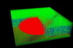
Image Caption: Atomistic structure of an artificial atom that could be used to produce light with vibrationally supressed fluctuations for quantum-enhanced sensors.
When this light is measured, this discrete or ‘granular’ nature leads to especially low fluctuations in its brightness, as two or more photons are never emitted at the same time.
This property is particularly useful in developing future quantum technologies, where low fluctuations are key, and has led to a surge of interest in engineered systems that act like atoms when they emit light, but whose properties are more easily tailored.
These ‘artificial atoms’ as they are known, are typically made from solid materials, and are in fact much larger objects, in which the presence of vibrations is unavoidable, and usually considered to be detrimental.
However, a collaborative team, led by the University of Bristol, has now established that these naturally occurring vibrations in artificial atoms can surprisingly lead to an even greater suppression of fluctuations in brightness than that present in natural atomic systems.
The authors, which include academics from the universities of Sheffield and Manchester, show that these low fluctuations could be used to build quantum sensors that are inherently more accurate than those possible without vibrations.
Dr Dara McCutcheon, principal investigator of the research and Lecturer in Quantum Engineering from the University of Bristol’s School of Physics said: “The implications of this research are quite far reaching.
“Usually one always thinks of the vibrations present in these relatively large artificial atoms as being detrimental to the light they emit, as typically the vibrations jostle the energy levels, with the resulting fluctuations imprinted onto the emitted photons.
“What’s happening here though, is that at low temperatures the vibrational environment acts to cool the system—in a sense freezing the energy levels, and in turn suppressing fluctuations on the emitted photons.”
This work points towards a new vision for these artificial atoms, in which their solid-state nature is actually put to good use to produce light that couldn’t be made using natural atomic systems.
It also opens the door to a new set of applications which use artificial atoms for quantum enhanced sensing, ranging from small scale magnetometry that could be used to measure signals in the brain, all the way up to full-scale gravitational wave detection revealing cosmic processes at the centre of galaxies.
Share on:


Subscribe
Stay ahead of the technologies shaping the future of electronics with our latest newsletter, Advanced Electronics Packaging Digest. Get expert insights on advanced packaging, materials, and system-level innovation, delivered straight to your inbox.
Subscribe now to stay informed, competitive, and connected.
Suggested Items
SMTA Ultra HDI Symposium, Day 1: AI at the Core or Out of the Game
04/13/2026 | Marcy LaRont, I-Connect007It was a beautiful 81°F morning in Arizona last Wednesday as I headed to the third annual SMTA Ultra HDI Symposium, focused on AI and ultra high density interconnect technology. Strategically held as part of Arizona’s Tech Week, this year’s conference took place in Avondale in Phoenix's West Valley. The event moved from the cozy offices of the Peoria Sports Complex (which paid homage to baseball’s spring training world) to the larger Avondale Conference Center, highlighting the importance of this area for electronics manufacturing investment.
PCBAA Sets Its Priorities for 2026: Support in the House and Senate
02/03/2026 | Marcy LaRont, I-Connect007David Schild, executive director of the Printed Circuit Board Association of America (PCBAA), leads an organization focused on the domestic manufacture of PCBs and substrates to support America’s critical microelectronics supply. In the continuation of this interview, David talks about the ways his organization is aligning its priorities with Washington, in particular, the Executive Branch. It might feel like a snail’s pace, but progress could mean financial support and more domestic security, even for the smaller companies.
SMT Perspectives & Prospects: Artificial Intelligence Part 6: Data Module 1
10/07/2025 | Dr. Jennie Hwang -- Column: SMT Perspectives and ProspectsData is one of the six pillars of AI infrastructure. It is critical to the performance of artificial intelligence (AI) models. AI data, essential to both the training and inference of Generative AI models, connotes the datasets used to train, validate, and test AI models. Training data provides models with a frame of reference by establishing a baseline against which models can compare new data using pre-trained models for predictions or generating new content.
U.S. Uses Secret Trackers to Trace AI Chips Diverted to China, Sources Say
08/18/2025 | I-Connect007 Editorial TeamTwo sources told Reuters that U.S. authorities have secretly placed location trackers in some advanced chip shipments they see as at high risk of illegal diversion to China. They said the trackers are intended to locate AI chips that are sent to locations restricted by U.S. export laws, but authorities only examine some shipments.
Happy’s Tech Talk #38: Novel Metallization for UHDI
05/07/2025 | Happy Holden -- Column: Happy’s Tech TalkI have been involved in high-density electronics substrates since 1970 when I joined Hewlett-Packard’s RF semiconductor group after college. Figure 1 shows the difference between trace/space lithography for substrates and silicon starting in 1970. My projects involved sapphire circuits for RF devices, but the figure displays the state of PCBs and integrated CMOS circuits and their packaging, not discreet RF devices. Even then, semiconductors were 50X higher density.