


 Dan’s Biz Bookshelf: ‘Abundance: How We Build a Better Future’
 Trouble in Your Tank: In Complex Systems, Design Rules Aren’t Optional
 It’s Only Common Sense: The Phone Is Still Your Competitive Advantage


Breakthrough Material Could Lead to Cheaper, More Widespread Solar Panels and Other Electronics
July 17, 2019 | The University of KansasEstimated reading time: 3 minutes
Imagine printing electronic devices using a simple inkjet printer — or even painting a solar panel onto the wall of a building.
Such technology would slash the cost of manufacturing electronic devices and enable new ways to integrate them into our everyday lives. Over the last two decades, a type of material called organic semiconductors, made out of molecules or polymers, has been developed for such purposes. But some properties of these materials pose a major hurdle that limits their widespread use.
“In these materials, an electron is usually bound to its counterpart, a missing electron known as ‘hole,’ and can’t move freely,” said Wai-Lun Chan, associate professor of physics & astronomy at the University of Kansas. “So-called ‘free electrons,’ which wander freely in the material and conduct electricity, are rare and can’t be generated readily by light absorption. This impedes the use of these organic materials in applications like solar panels because panels built with these materials often have poor performance.”
Because of this problem, Chan said “freeing the electrons” has been a focus in developing organic semiconductors for solar cells, light sensors and many other optoelectronic applications.
Now, two physics research groups at KU, led by Chan and Hui Zhao, professor of physics & astronomy, have effectively generated free electrons from organic semiconductors when combined with a single atomic layer of molybdenum disulfide (MoS2), a recently discovered two-dimensional (2D) semiconductor.
The introduced 2D layer allows the electrons to escape from “holes” and move freely. The findings have just been published in the Journal of American Chemical Society, a leading journal in chemistry and interfacing areas of science.
Over the last few years, many researchers have been investigating how free charges can be generated effectively from hybrid organic-2D interfaces.
“One of the prevailing assumptions is free electrons can be generated from the interface as long as electrons can be transferred from one material to another in a relatively short period of time — less than one-trillionth of a second,” Chan said. “However, my graduate students Tika Kafle and Bhupal Kattel and I have found the presence of the ultrafast electron transfer in itself is not sufficient to guarantee the generation of free electrons from the light absorption. That’s because the ‘holes’ can prevent the electrons from moving away from the interface. Whether the electron can be free from this binding force depends on the local energy landscape near the interface.”
Chan said the energy landscape of the electrons could be seen as a topographic map of a mountain.
“A hiker chooses his path based on the height contour map,” he said. “Similarly, the motion of the electron at the interface between the two materials is controlled by the electron energy landscape near the interface.”
Chan and Zhao’s findings will help develop general principles of how to design the “landscape” to free the electrons in such hybrid materials.
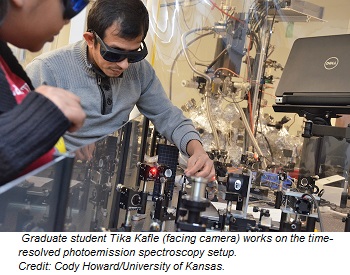
The discovery was made by combining two highly complementary experimental tools based on ultrafast lasers, time-resolved photoemission spectroscopy in Chan's lab and transient optical absorption in Zhao's lab. Both experimental setups are located in the basement of the Integrated Science Building.
In the time-resolved photoemission spectroscopy experiment, Kafle used an ultrashort laser pulse that only exists for 10-quadrillionths (10-14) of a second to trigger the motion of electrons. The advantage of using such a short pulse is the researcher knows precisely the starting time of the electron’s journey. Kafle then used another ultrashort laser pulse to hit the sample again at an accurately controlled time relative to the first pulse. This second pulse is energetic enough to kick out these electrons from the sample. By measuring the energy of these electrons (now in a vacuum) and using the principle of energy conservation, the researchers were able to figure out the energy of electrons before they were kicked out and thus reveal the journey of these electrons since they were hit by the first pulse. This technique resolved the energy of the excited electrons as it moves across the interface after the light absorption. Because only electrons near the front surface of the sample can be released by the second pulse, the position of the electron relative to the interface is also revealed with atomic precision.
In the transient optical absorption measurements, Peng Yao (a visiting student) and KU graduate Peymon Zereshki, both supervised by Zhao, also used a two-pulse technique, with the first pulse initiating the electron motion in the same way. However, in their measurements, the second pulse does the trick of monitoring electrons by detecting the fraction of the second pulse that is reflected from the sample, instead of kicking out the electrons.
“Because light can penetrate a longer distance, the measurement can probe electrons in the entire depth of the sample and therefore provide complementary information to the first techniques that are more ‘surface sensitive,’” Zhao said. “These detailed measurements enabled us to reconstruct the trajectory of the electron and determine conditions that enable the effective generation of free electrons.”
The collaborative work from the two research teams will provide a blueprint on how to design interfaces that can turn light into electrical current with high efficiency. Both teams are funded by the National Science Foundation through a CAREER Award (Chan) and a Condensed Matter Physics Award (Zhao).
Share on:


Subscribe
Stay ahead of the technologies shaping the future of electronics with our latest newsletter, Advanced Electronics Packaging Digest. Get expert insights on advanced packaging, materials, and system-level innovation, delivered straight to your inbox.
Subscribe now to stay informed, competitive, and connected.
Suggested Items
AI Demand Drives PCB Material Market Growth
05/08/2026 | TPCAAs AI computing continues to drive a comprehensive upgrade in hardware specifications, the global printed circuit board industry is undergoing a profound structural transformation.
I-Connect007 Editor’s Choice: Five Must-Reads for the Week
05/01/2026 | Michelle Te, I-Connect007If it feels like the PCB industry is accelerating faster than ever, you’re not imagining it. From advanced materials driven by AI applications to renewed investment in domestic manufacturing—and the next generation stepping into critical roles—there’s a lot shifting at once. My selections for this week highlight where the pressure points are forming, and where the opportunities are emerging.
Electronics Manufacturing Needs Your Voice: Global Sentiment Survey Now Live
04/30/2026 | Global Electronics AssociationThe latest monthly Global Sentiment Survey from the Global Electronics Association is now open. At a time when demand uncertainty, policy shifts, energy costs, and supply chain recalibration are pulling the industry in multiple directions, the survey captures something macroeconomic data often misses: how manufacturers are actually experiencing conditions on the ground.
From Backbone to Breakthroughs: I-Connect007 Wraps PCB Materials Series with Focus on Innovation
05/06/2026 | I-Connect007I-Connect007 wraps up its six-part podcast series, PCB Materials: The Backbone and Future of Electronics, with Episode 6 and a discussion focusing on innovation. In Episode 6, Marcy LaRont speaks with Isola CTO Kirk Thompson about a critical turning point for the PCB industry as innovation accelerates. As data rates climb and demands from AI infrastructure, power density, flexible electronics, photonics, and chiplet integration intensify, traditional material assumptions are no longer sufficient.
Jiva Soluboard Getting the Attention It Deserves
04/30/2026 | Marcy LaRont, I-Connect007 MagazineJiva is a newer company that bridges the divide between PCB fabrication and product circularity or sustainability. Jiva Soluboard is the first fully recyclable laminate material ever created for PCB fabrication, and it's not going unnoticed. Stephen Driver, CEO of Jiva, gave us an update at APEX EXPO, including an exciting certification achievement in February.